SWRA729 April   2022 CC1352P , CC2652P


  1.   Trademarks
  2.   Acronyms
  3. 1Reference Designs Available
    1. 1.1 Single Component for 10-dBm PA Port
      1. 1.1.1 Murata PA IPC Equivalent Circuit
      2. 1.1.2 IPC Size and Dimensions
    2. 1.2 CC2652P PA IPC EM
      1. 1.2.1 Component Placement and Layout
      2. 1.2.2 Layout - Layer 1
      3. 1.2.3 Layout - Layer 2
      4. 1.2.4 Layout - Layer 3
      5. 1.2.5 Layout - Layer 4
  4. 2PA IPC Measurement Results
    1. 2.1 CC2652P Output Power, 1-Mbps Bluetooth Low Energy
    2. 2.2 CC2652P TX Efficiency, Harmonics, and Output Power at Various PA Settings
  5. 3Harmonic Emission Regulatory Requirements
    1. 3.1 Compliance with FCC regulations
    2. 3.2 Compliance with Regulations
  6. 4Summary
  7. 5References

Layout - Layer 3

Figure 1-9 shows the third layer of the 4-layer reference design. This layer is mainly for VDDS and VDDR power. Remaining area is filled with GND for shielding purposes. The power routing should always be routed to the decoupling capacitor first; then from the decoupling capacitor to the pad of the CC2652P.
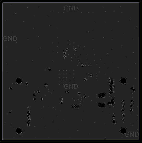
GUID-20211124-SS0I-JHBS-ZXW7-MB082ZQXHQLP-low.pngFigure 1-9 Layer 3