TIDUEY6 April 2021
- Description
- Resources
- Features
- Applications
- 5
- 1System Description
- 2System Overview
-
3Hardware, Software, Testing Requirements, and Test Results
- 3.1
Hardware Requirements
- 3.1.1
Hardware Overview
- 3.1.1.1
Control Module
- 3.1.1.1.1
Control Mother Board
- 3.1.1.1.1.1 Inverter Safing - UCC5870 ASC and Fault Control
- 3.1.1.1.1.2 DC-DC Safing
- 3.1.1.1.1.3 DC-DC Converter Secondary PWM Selection
- 3.1.1.1.1.4 Blower Fan Control
- 3.1.1.1.1.5 Voltage Monitor
- 3.1.1.1.1.6 Resolver Interface Control
- 3.1.1.1.1.7 Test Points on Control Module
- 3.1.1.1.1.8 General Purpose Ports
- 3.1.1.1.1.9 Connectors and Headers on Control Mother Board
- 3.1.1.1.2 Power Supplies
- 3.1.1.1.3 TCAN4550 module
- 3.1.1.1.4 Dual TCAN Module
- 3.1.1.1.5 Analog Back End Module
- 3.1.1.1.6 Resolver Analog Front End Module
- 3.1.1.1.1
Control Mother Board
- 3.1.1.2 Inverter Module
- 3.1.1.3 DC-DC Bidirectional Converter Module
- 3.1.1.1
Control Module
- 3.1.1
Hardware Overview
- 3.2 Resource Mapping
- 3.3 Test Setup
- 3.4 Test Results
- 3.1
Hardware Requirements
- 4General Texas Instruments High Voltage Evaluation (TI HV EVM) User Safety Guidelines
- 5Design and Documentation Support
- 6About the Author
3.1.1.1.1.2 DC-DC Safing
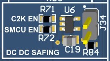
DC-DC converter deals with high voltages and currents and a safe operation of the converter for assumed safety goals is critical to ASIL D compliance. In the event of an over voltage detected in the converter, it is designed to be shut down. The safety MCU will monitor the safe operation of DC-DC converter and send the shut down signals as needed. In the event of PMIC device on the safety MCU control card determining unsafe power levels, it can also shut down the converter. However, during development and testing, C2000 MCU may be needed to generate the shut down signal. The choice between C2000 and safety MCU can be made by selection of 0E resistors, R71 and R72 respectively, on the control mother board. This section of the board is shown in Figure 3-5.
 Figure 3-5 MCU Selection
for DC-DC Safing
Figure 3-5 MCU Selection
for DC-DC Safing- DO NOT populate resistors R71 and R72 at the same time as that will tie the outputs of two MCUs together. If they were configured for different polarities, it may damage the output pins of MCUs tied to these resistors.
- If jumper J34 is removed, then it will continuously enable the converter. This can be used during low votlage debug times. When full operation is required, this jumper must be populated.