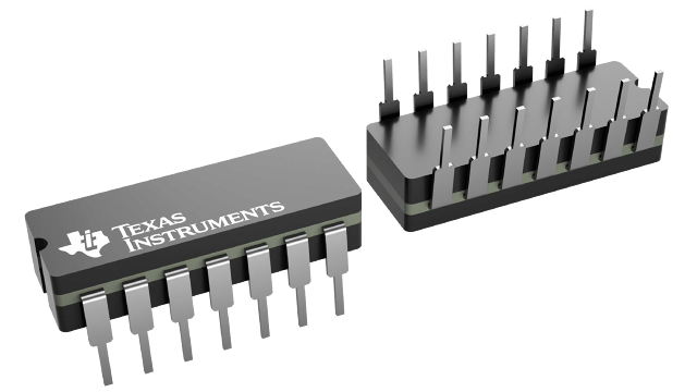
Packaging information
| Package | Pins CDIP (J) | 14 |
| Operating temperature range (°C) -55 to 125 |
| Package qty | Carrier 25 | TUBE |
Features for the CD54HC164
- Buffered inputs
- Asynchronous reset
- Typical fMAX = 60MHz at VCC = 5V, CL = 15pF, TA = 25°C
- Fanout (overtemperature range)
- Standard Outputs: 10 LSTTL loads
- Bus driver outputs: 15 LSTTL loads
- Wide operating temp range: – 55°C to 125°C
- Balanced propagation delay and transition times
- Significant power reduction compared to LSTTL logic ICs
- HC types
- 2V to 6V operation
- High noise immunity: NIL = 30%, NIH = 30% of VCC at VCC = 5V
- HCT types
- 4.5V to 5.5V operation
- Direct LSTTL input logic compatibility, VIL = 0.8V (Max), VIH = 2V (Min)
- CMOS input compatibility, II ≤ 1µA at VOL, VOH
Description for the CD54HC164
The ’HC164 and ’HCT164 are 8-bit, serial-in, parallel-out, shift registers with asynchronous reset. Data is shifted on the positive edge of Clock (CLK). A LOW on the RESET (CLR) pin resets the shift register and all outputs go to the LOW state regardless of the input conditions. Two Serial Data inputs (A and B) are provided, either one can be used as a data enable control.
