パッケージ情報
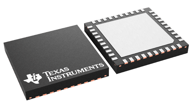
| パッケージ | ピン数 WQFN (RTA) | 40 |
| 動作温度範囲 (℃) -40 to 85 |
| パッケージ数量 | キャリア 2,500 | LARGE T&R |
DS25BR440 の特徴
- DC - 3.125 Gbps Low Jitter, Low Skew, Low Power Operation
- Pin Selectable Transmit Pre-Emphasis and Receive Equalization Eliminate Data Dependant Jitter
- Wide Input Common Mode Voltage Range Allows DC-Coupled Interface to LVDS, CML and LVPECL Drivers
- LOS Circuitry Detects Open Inputs Fault
- Integrated 100Ω Input and Output Terminations
- 8 kV ESD on LVDS I/O Pins Protects Adjoining Components
- Small 6 mm x 6 mm WQFN-40 Space Saving Package
All trademarks are the property of their respective owners.
DS25BR440 に関する概要
The DS25BR440 is a 3.125 Gbps Quad LVDS buffer optimized for high-speed signal routing and repeating over lossy FR-4 printed circuit board backplanes and balanced cables. Fully differential signal paths ensure exceptional signal integrity and noise immunity.
The DS25BR440 features two levels of transmit pre-emphasis (PE) and two levels of receive equalization (EQ). Both of these features compensate for interconnect losses and ultimately maximize noise margin. A loss-of-signal (LOS) circuit monitors each input channel and a unique LOS pin is asserted when no signal is detected at that input.
Wide input common mode range allows the switch to accept signals with LVDS, CML and LVPECL levels; the output levels are LVDS. A very small package footprint requires a minimal space on the board while the flow-through pinout allows easy board layout. Each differential input and output is internally terminated with a 100Ω resistor to lower device return losses, reduce component count and further minimize board space.