パッケージ情報
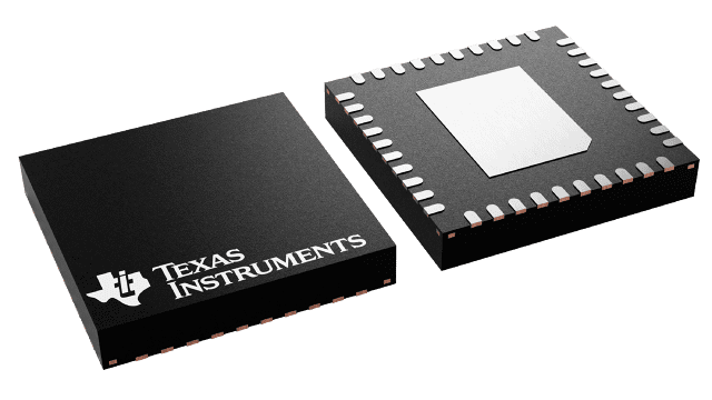
| パッケージ | ピン数 VQFN (RHA) | 40 |
| 動作温度範囲 (℃) -40 to 125 |
| パッケージ数量 | キャリア 2,500 | LARGE T&R |
TPS65287 の特徴
- Wide Input Supply Voltage Range:
4.5 V – 18 V - 0.8-V, 1% Accuracy Reference
- Continuous Loading:
3 A (Buck1), 2 A (Buck2 and 3) - Maximum Current:
3.5 A (Buck 1), 2.5 A (Buck2 and 3) - 300-kHz – 2.2-MHz Switching
Frequency Set By External Resistor - External Enable Pins With Built-In Current
Source for Easy Sequencing - External Soft Start Pins
- Adjustable Cycle-by-Cycle Current Limit
Set by External Resistor - Current-Mode Control With Simple Compensation Circuit
- Pulse Skipping Mode to Achieve High Light Load Efficiency,
Allowing for an Output Ripple Better than 2% - Support Pre-Biased Outputs
- Power Good Supervisor and Reset Generator
- Up to 2.1-A USB Power With Over Current Setting by
External Resistor - Individual Thermal Protection for USB Switch
- Push Button (10-kV ESD Rated Pin for PB_IN) Control
for Intelligent System Power-On/Power-Off Operation - Small, Thermally Efficient 40-Pin 6-mm × 6-mm RHA (QFN)
package - –40°C to 125°C Junction Temperature Range
TPS65287 に関する概要
TPS65287 is a power management IC with three step-down buck converters. Both high-side and low-side MOSFETs are integrated to provide fully synchronous conversion with higher efficiency. The converters are designed to simplify its application while giving the designer the option to optimize their usage according to the target application.
The converters can operate in 5-, 9-, 12- or 15-V systems. The output voltage can be set externally using a resistor divider to any value between 0.8 V and the input supply minus the resistive drops on the converter path. Each converter features enable pin that allows a delayed start-up for sequencing purposes, soft start pin that allows adjustable soft-start time by choosing the soft-start capacitor, and a current limit (RLIM) pin that enables designer to adjust current limit by selecting an external resistor and optimize the choice of inductor. All converters operate in ‘hiccup mode’: Once an over-current lasting more than 10 ms is sensed in any of the converters, they will shut down for 10 ms and then the start-up sequencing will be tried again. If the overload has been removed, the converter will ramp up and operate normally. If this is not the case the converter will see another over-current event and shuts down again repeating the cycle (hiccup) until the failure is cleared. If an overload condition lasts for less than 10 ms, only the relevant converter affected will shut-down and re-start and no global hiccup mode will occur.
The switching frequency of the converters is set by an external resistor connected to ROSC pin. The switching regulators are designed to operate from 300 kHz to 2.2 MHz. The converters operate with 180° phase between then to minimize the input filter requirements.
All converters have peak current mode control which simplifies external frequency compensation. The device has a built-in slope compensation ramp. The slope compensation can prevent sub harmonic oscillations in peak current mode control. A traditional type II compensation network can stabilize the system and achieve fast transient response. Moreover, an optional capacitor in parallel with the upper resistor of the feedback divider provides one more zero and makes the crossover frequency over 100 kHz.
All converters feature an automatic low power pulse PFM skipping mode which improves efficiency during light loads and standby operation, while guaranteeing a very low output ripple, allowing for a value of less than 2% at low output voltages.
The device incorporates an overvoltage transient protection circuit to minimize voltage overshoot. The OVP feature minimizes the output overshoot by implementing a circuit to compare the FB pin voltage to OVP threshold which is 106% of the internal voltage reference. If the FB pin voltage is greater than the OVTP threshold, the high side MOSFET is disabled preventing current from flowing to the output and minimizing output overshoot. When the FB voltage drops lower than the OVP lower threshold which is 104%, the high side MOSFET is allowed to turn on the next clock cycle.
TPS65287 features a supervisor circuit which monitors each buck’s output and the PGOOD pin is asserted once sequencing is done. The PGOOD pin is an open drain output. The PGOOD pin is pulled low when any buck converter is pulled below 85% of the nominal output voltage. The PGOOD is pulled up when all converter outputs are more than 90% of its nominal output voltage. The default reset time is 100 ms. The polarity of the PGOOD is active high.
The push button operation has been designed to allow for automatic system start when the input supply is applied or to provide an integrated ON/OFF system management without the need of additional external components. The behavior of the device will depend on the status of the INT pin (see start-up signals).
The USB switch provides up to 2.1-A of current as required by downstream USB devices and setting by external resistor. When the output load exceeds the current-limit threshold or a short is present, the PMU limits the output current to a safe level by switching into a constant-current mode and pulling the over current logic output low. When continuous heavy overloads and short circuits increase the power dissipation in the switch, causing the junction temperature to rise, a thermal warning protection circuit shuts off the USB switch and allows the buck converters to carry on operating.
The device implements an internal thermal shutdown to protect itself if the junction temperature exceeds 160°C. The thermal shutdown forces the device to stop operating when the junction temperature exceeds thermal trip threshold. Once the die temperature decreases below 140°C, the device reinitiates the power up sequence. The thermal shutdown hysteresis is 20°C.