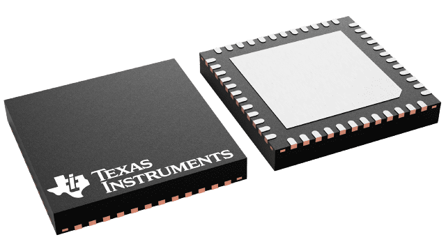
Packaging information
| Package | Pins VQFN (RGZ) | 48 |
| Operating temperature range (°C) -40 to 85 |
| Package qty | Carrier 2,500 | LARGE T&R |
Features for the MSP430F5224
- Dual-Supply Voltage Device
- Primary Supply (AVCC,
DVCC):
- Powered From External Supply:
3.6 V Down to 1.8 V - Up to 22 General-Purpose I/Os With up to Four External Interrupts
- Powered From External Supply:
- Low-Voltage Interface Supply
(DVIO):
- Powered From Separate External Supply: 1.62 V to 1.98 V
- Up to 31 General-Purpose I/Os With up to 12 External Interrupts
- Serial Communications
- Primary Supply (AVCC,
DVCC):
- Ultra-Low Power Consumption
- Active Mode (AM):
All System Clocks Active
290 µA/MHz at 8 MHz, 3.0 V, Flash Program Execution (Typical)
150 µA/MHz at 8 MHz, 3.0 V, RAM Program Execution (Typical) - Standby Mode (LPM3):
Real-Time Clock (RTC) With Crystal, Watchdog, and Supply Supervisor Operational, Full RAM Retention, Fast Wakeup:
1.9 µA at 2.2 V, 2.1 µA at 3.0 V (Typical)
Low-Power Oscillator (VLO), General-Purpose Counter, Watchdog, and Supply Supervisor Operational, Full RAM Retention, Fast Wakeup:
1.4 µA at 3.0 V (Typical) - Off Mode (LPM4):
Full RAM Retention, Supply Supervisor Operational, Fast Wakeup:
1.1 µA at 3.0 V (Typical) - Shutdown Mode (LPM4.5):
0.18 µA at 3.0 V (Typical)
- Active Mode (AM):
- Wake up From Standby Mode in 3.5 µs (Typical)
- 16-Bit RISC Architecture, Extended Memory, up to 25-MHz System Clock
- Flexible Power-Management System
- Fully Integrated LDO With Programmable Regulated Core Supply Voltage
- Supply Voltage Supervision, Monitoring, and Brownout
- Unified Clock System
- FLL Control Loop for Frequency Stabilization
- Low-Power Low-Frequency Internal Clock Source (VLO)
- Low-Frequency Trimmed Internal Reference Source (REFO)
- 32-kHz Watch Crystals (XT1)
- High-Frequency Crystals up to 32 MHz (XT2)
- 16-Bit Timer TA0, Timer_A With Five Capture/Compare Registers
- 16-Bit Timer TA1, Timer_A With Three Capture/Compare Registers
- 16-Bit Timer TA2, Timer_A With Three Capture/Compare Registers
- 16-Bit Timer TB0, Timer_B With Seven Capture/Compare Shadow Registers
- Two Universal Serial Communication Interfaces
- USCI_A0 and USCI_A1 Each Support:
- Enhanced UART With Automatic Baud Rate Detection
- IrDA Encoder and Decoder
- Synchronous SPI
- USCI_B0 and USCI_B1 Each Support:
- I2C
- Synchronous SPI
- USCI_A0 and USCI_A1 Each Support:
- 10-Bit Analog-to-Digital Converter (ADC) With Internal Reference, Sample-and-Hold
- Comparator
- Hardware Multiplier Supports 32-Bit Operations
- Serial Onboard Programming, No External Programming Voltage Needed
- Three-Channel Internal DMA
- Basic Timer With RTC Feature
- Device Comparison Summarizes Available Family Members
Description for the MSP430F5224
The TI MSP430™ family of ultra-low-power microcontrollers consists of several devices featuring different sets of peripherals targeted for various applications. The architecture, combined with extensive low-power modes, is optimized to achieve extended battery life in portable measurement applications. The device features a powerful 16-bit RISC CPU, 16-bit registers, and constant generators that contribute to maximum code efficiency. The digitally controlled oscillator (DCO) allows the device to wake up from low-power modes to active mode in 3.5 µs (typical).
The MSP430F522x series are microcontrollers with four 16-bit timers, a high-performance 10-bit ADC, two universal serial communication interfaces (USCIs), a hardware multiplier, DMA, a comparator, and an RTC module with alarm capabilities.
The MSP430F521x series include all of the peripherals of the MSP430F522x series with the exception of the ADC.
All devices have a split I/O supply system that allows for a seamless interface to other devices that have a nominal 1.8-V I/O interface without the need for external level translation.
For complete module descriptions, see the MSP430F5xx and MSP430F6xx Family User’s Guide. For design guidelines, see Designing With MSP430F522x and MSP430F521x Devices.