SLASE67A January 2015 – August 2019 ADS54J54
PRODUCTION DATA.
- 1 Features
- 2 Applications
- 3 Description
- 4 Revision History
- 5 Pin Configuration and Functions
-
6 Specifications
- 6.1 Absolute Maximum Ratings
- 6.2 ESD Ratings
- 6.3 Recommended Operating Conditions
- 6.4 Thermal Information
- 6.5 Electrical Characteristics
- 6.6 Electrical Characteristics: 250 MSPS Output, 2x Decimation Filter
- 6.7 Electrical Characteristics: 500 MSPS Output
- 6.8 Electrical Characteristics: Sample Clock Timing Characteristics
- 6.9 Electrical Characteristics: Digital Outputs
- 6.10 Timing Requirements
- 6.11 Reset Timing
- 6.12 Typical Characteristics
-
7 Detailed Description
- 7.1 Overview
- 7.2 Functional Block Diagram
- 7.3
Feature Description
- 7.3.1 Decimation by 2 (250 MSPS Output)
- 7.3.2 Over-Range Indication
- 7.3.3 JESD204B Interface
- 7.3.4 SYSREF Clocking Schemes
- 7.3.5 Split-Mode Operation
- 7.3.6 Eye Diagram Information
- 7.3.7 Analog Inputs
- 7.3.8 Clock Inputs
- 7.3.9 Input Clock Divider
- 7.3.10 Power-Down Control
- 7.3.11 Device Configuration
- 7.3.12 JESD204B Interface Initialization Sequence
- 7.3.13 Device and Register Initialization
- 7.4 Device Functional Modes
- 7.5 Programming
- 7.6
Register Maps
- 7.6.1
Register Descriptions
- 7.6.1.1 Register Address 0
- 7.6.1.2 Register Address 1
- 7.6.1.3 Register Address 3
- 7.6.1.4 Register Address 4
- 7.6.1.5 Register Address 5
- 7.6.1.6 Register Address 6
- 7.6.1.7 Register Address 7
- 7.6.1.8 Register Address 8
- 7.6.1.9 Register Address 12
- 7.6.1.10 Register Address 13
- 7.6.1.11 Register Address 14
- 7.6.1.12 Register Address 15
- 7.6.1.13 Register Address 16
- 7.6.1.14 Register Address 19
- 7.6.1.15 Register Address 22
- 7.6.1.16 Register Address 23
- 7.6.1.17 Register Address 26
- 7.6.1.18 Register Address 29
- 7.6.1.19 Register Address 30
- 7.6.1.20 Register Address 31
- 7.6.1.21 Register Address 32
- 7.6.1.22 Register Address 33
- 7.6.1.23 Register Address 99
- 7.6.1.24 Register Address 100
- 7.6.1.25 Register Address 103
- 7.6.1.26 Register Address 104
- 7.6.1.27 Register Address 107
- 7.6.1.28 Register Address 108
- 7.6.1
Register Descriptions
- 8 Application and Implementation
- 9 Power Supply Recommendations
- 10Layout
- 11Device and Documentation Support
- 12Mechanical, Packaging, and Orderable Information
Package Options
Mechanical Data (Package|Pins)
- RGC|64
Thermal pad, mechanical data (Package|Pins)
- RGC|64
Orderable Information
8.4.1 SNR and Clock Jitter
The signal-to-noise ratio of the channel is limited by three different factors: the quantization noise is typically not noticeable in pipeline converters and is 84 dB for a 14-bit channel. The thermal noise limits the SNR at low input frequencies while the clock jitter sets the SNR for higher input frequencies.

Calculate the SNR limitation due to sample clock jitter using the following:

The total clock jitter (tJitter) has two components – the internal aperture jitter (98 fs for ADS54J54), which is set by the noise of the clock input buffer, the external clock jitter, and the jitter from the analog input signal. Calculate total clock jitter using the following:

External clock jitter can be minimized by using high quality clock sources and jitter cleaners, as well as bandpass filters at the clock input while a faster clock slew rate improves the channel aperture jitter.
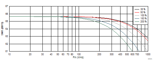
The ADS54J54 has a thermal noise of 66 dBFS and internal aperture jitter of 98 fs. The SNR depending on amount of external jitter for different input frequencies is shown in Figure 103.
