SNVSAU8A June 2017 – February 2024 TPS549B22
PRODUCTION DATA
- 1
- 1 Features
- 2 Applications
- 3 Description
- 4 Pin Configuration and Functions
- 5 Specifications
-
6 Detailed Description
- 6.1 Overview
- 6.2 Functional Block Diagram
- 6.3 Feature Description
- 6.4 Device Functional Modes
- 6.5 Programming
-
7 Register Maps
- 7.1 OPERATION Register (address = 1h)
- 7.2 ON_OFF_CONFIG Register (address = 2h)
- 7.3 CLEAR FAULTS (address = 3h)
- 7.4 WRITE PROTECT (address = 10h)
- 7.5 STORE_DEFAULT_ALL (address = 11h)
- 7.6 RESTORE_DEFAULT_ALL (address = 12h)
- 7.7 CAPABILITY (address = 19h)
- 7.8 VOUT_MODE (address = 20h)
- 7.9 VOUT_COMMAND (address = 21h)
- 7.10 VOUT_MARGIN_HIGH (address = 25h) ®
- 7.11 VOUT_MARGIN_LOW (address = 26h)
- 7.12 STATUS_BYTE (address = 78h)
- 7.13 STATUS_WORD (High Byte) (address = 79h)
- 7.14 STATUS_VOUT (address = 7Ah)
- 7.15 STATUS_IOUT (address = 7Bh)
- 7.16 STATUS_CML (address = 7Eh)
- 7.17 MFR_SPECIFIC_00 (address = D0h)
- 7.18 MFR_SPECIFIC_01 (address = D1h)
- 7.19 MFR_SPECIFIC_02 (address = D2h)
- 7.20 MFR_SPECIFIC_03 (address = D3h)
- 7.21 MFR_SPECIFIC_04 (address = D4h)
- 7.22 MFR_SPECIFIC_06 (address = D6h)
- 7.23 MFR_SPECIFIC_07 (address = D7h)
- 7.24 MFR_SPECIFIC_44 (address = FCh)
-
8 Application and Implementation
- 8.1 Application Information
- 8.2
Typical Applications
- 8.2.1 TPS549B22 1.5-V to 18-V Input, 1-V Output, 25-A Converter
- 8.2.2 Design Requirements
- 8.2.3
Detailed Design Procedure
- 8.2.3.1 Custom Design With WEBENCH® Tools
- 8.2.3.2 Switching Frequency Selection
- 8.2.3.3 Inductor Selection
- 8.2.3.4 Output Capacitor Selection
- 8.2.3.5 Input Capacitor Selection
- 8.2.3.6 Bootstrap Capacitor Selection
- 8.2.3.7 BP Pin
- 8.2.3.8 R-C Snubber and VIN Pin High-Frequency Bypass
- 8.2.3.9 Optimize Reference Voltage (VSEL)
- 8.2.3.10 MODE Pin Selection
- 8.2.3.11 ADDR Pin Selection
- 8.2.3.12 Overcurrent Limit Design
- 8.2.4 Application Curves
- 8.3 Power Supply Recommendations
- 8.4 Layout
- 9 Device and Documentation Support
- 10Revision History
- 11Mechanical, Packaging, and Orderable Information
Package Options
Refer to the PDF data sheet for device specific package drawings
Mechanical Data (Package|Pins)
- RVF|40
Thermal pad, mechanical data (Package|Pins)
- RVF|40
Orderable Information
8.2.3.3 Inductor Selection
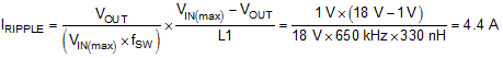
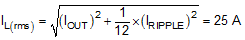
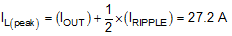
To calculate the value of the output inductor, use Equation 3. The coefficient KIND represents the amount of inductor ripple current relative to the maximum output current. The output capacitor filters the inductor ripple current. Therefore, choosing a high inductor ripple current impacts the selection of the output capacitor because the output capacitor must have a ripple current rating equal to or greater than the inductor ripple current. In general, maintain a KIND coefficient between 0 and 40 for balanced performance. Using this target ripple current, the required inductor size can be calculated as shown in Equation 3
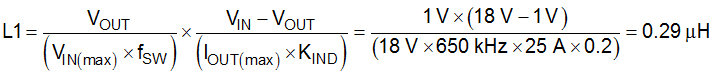
Selecting a KIND of 0.2, the target inductance L1 = 290 nH. Using the next standard value, the 330 nH is chosen in this application for the high current rating, low DCR, and small size. The inductor ripple current, RMS current, and peak current can be calculated using Equation 4, Equation 5 and Equation 6. Use these values to select an inductor with approximately the target inductance value, and current ratings that allow normal operation with some margin.