SNVSAU8A June 2017 – February 2024 TPS549B22
PRODUCTION DATA
- 1
- 1 Features
- 2 Applications
- 3 Description
- 4 Pin Configuration and Functions
- 5 Specifications
-
6 Detailed Description
- 6.1 Overview
- 6.2 Functional Block Diagram
- 6.3 Feature Description
- 6.4 Device Functional Modes
- 6.5 Programming
-
7 Register Maps
- 7.1 OPERATION Register (address = 1h)
- 7.2 ON_OFF_CONFIG Register (address = 2h)
- 7.3 CLEAR FAULTS (address = 3h)
- 7.4 WRITE PROTECT (address = 10h)
- 7.5 STORE_DEFAULT_ALL (address = 11h)
- 7.6 RESTORE_DEFAULT_ALL (address = 12h)
- 7.7 CAPABILITY (address = 19h)
- 7.8 VOUT_MODE (address = 20h)
- 7.9 VOUT_COMMAND (address = 21h)
- 7.10 VOUT_MARGIN_HIGH (address = 25h) ®
- 7.11 VOUT_MARGIN_LOW (address = 26h)
- 7.12 STATUS_BYTE (address = 78h)
- 7.13 STATUS_WORD (High Byte) (address = 79h)
- 7.14 STATUS_VOUT (address = 7Ah)
- 7.15 STATUS_IOUT (address = 7Bh)
- 7.16 STATUS_CML (address = 7Eh)
- 7.17 MFR_SPECIFIC_00 (address = D0h)
- 7.18 MFR_SPECIFIC_01 (address = D1h)
- 7.19 MFR_SPECIFIC_02 (address = D2h)
- 7.20 MFR_SPECIFIC_03 (address = D3h)
- 7.21 MFR_SPECIFIC_04 (address = D4h)
- 7.22 MFR_SPECIFIC_06 (address = D6h)
- 7.23 MFR_SPECIFIC_07 (address = D7h)
- 7.24 MFR_SPECIFIC_44 (address = FCh)
-
8 Application and Implementation
- 8.1 Application Information
- 8.2
Typical Applications
- 8.2.1 TPS549B22 1.5-V to 18-V Input, 1-V Output, 25-A Converter
- 8.2.2 Design Requirements
- 8.2.3
Detailed Design Procedure
- 8.2.3.1 Custom Design With WEBENCH® Tools
- 8.2.3.2 Switching Frequency Selection
- 8.2.3.3 Inductor Selection
- 8.2.3.4 Output Capacitor Selection
- 8.2.3.5 Input Capacitor Selection
- 8.2.3.6 Bootstrap Capacitor Selection
- 8.2.3.7 BP Pin
- 8.2.3.8 R-C Snubber and VIN Pin High-Frequency Bypass
- 8.2.3.9 Optimize Reference Voltage (VSEL)
- 8.2.3.10 MODE Pin Selection
- 8.2.3.11 ADDR Pin Selection
- 8.2.3.12 Overcurrent Limit Design
- 8.2.4 Application Curves
- 8.3 Power Supply Recommendations
- 8.4 Layout
- 9 Device and Documentation Support
- 10Revision History
- 11Mechanical, Packaging, and Orderable Information
Package Options
Refer to the PDF data sheet for device specific package drawings
Mechanical Data (Package|Pins)
- RVF|40
Thermal pad, mechanical data (Package|Pins)
- RVF|40
Orderable Information
5.6 Typical Characteristics
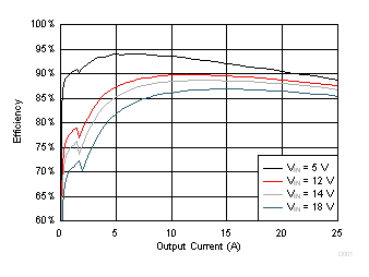
| VOUT = 1 V | VDD = VIN | SKIP Mode |
| fSW = 650 kHz |
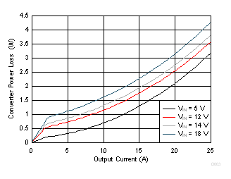
| VOUT = 1 V | VDD= VIN | SKIP Mode |
| fSW = 650 kHz |
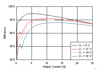
| VDD = VIN | fSW = 650 kHz | SKIP Mode |
| VOUT = 2.5 V | L= 820 nH, 0.9 mΩ |
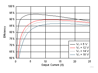
| VOUT = 1 V | VDD = VIN | FCCM Mode |
| fSW = 650 kHz |
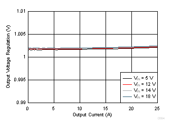
| VOUT = 1 V | VDD = VIN | FCCM Mode |
| fSW = 650 kHz |
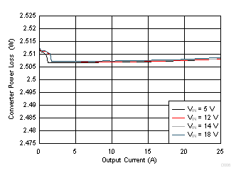
| VDD = VIN | fSW = 650 kHz | SKIP Mode |
| VOUT = 2.5 V | L= 820 nH, 0.9 mΩ |
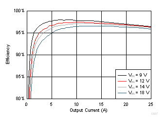
| VDD = VIN | fSW = 650 kHz | FCCM Mode |
| VOUT = 5 V | L= 820 nH, 0.9 mΩ |
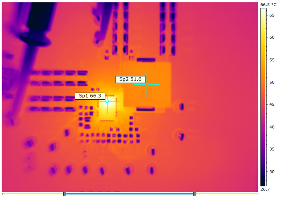
| VDD = VIN = 12 V | fSW = 650 kHz | IOUT = 25 A |
| VOUT = 1 V | Natural convection at room temperature | |
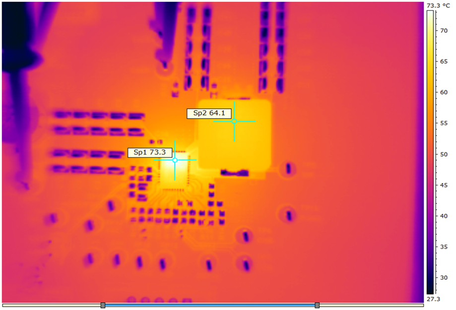
| VDD = VIN = 12 V | fSW = 650 kHz | IOUT = 25 A |
| VOUT = 2.5 V | Natural convection at room temperature | |
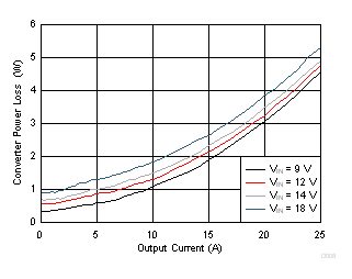
| VDD = VIN | fSW = 650 kHz | FCCM Mode |
| VOUT = 5 V | L= 820 nH, 0.9 mΩ | |
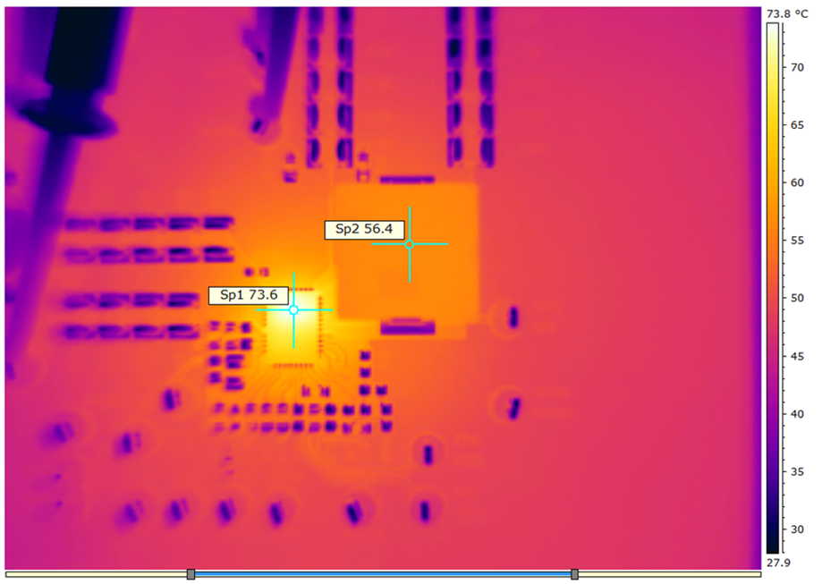
| VDD = VIN = 12 V | fSW = 650 kHz | IOUT = 25 A |
| VOUT = 1 V | Natural convection at room temperature | |
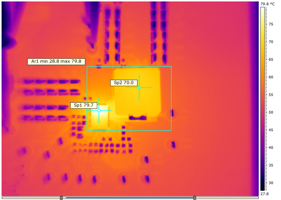
| VDD = VIN = 12 V | fSW = 650 kHz | IOUT = 25 A |
| VOUT = 5 V | Natural convection at room temperature | |
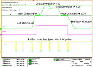 Figure 5-13 PMBus 1-MHz Bus Speed with 1.8-V Pullup
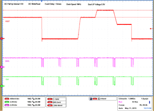
| 1 – Operation only | 4 – VOUT Command up to 1.2 V | |||
| 2 – Turnoff | 5 – VOUT Command down to 0.6 V | |||
| 3 – Turnon without Margin | 6 – Turnoff | |||
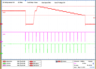
| 1 – Operation only | 4 – 16 VOUT Command up to 1.2 V, | |||
| 2 – Turnoff | 50 mV per step down to 0.6 V | |||
| 3 – Turnon without Margin | 17 – Turnoff | |||
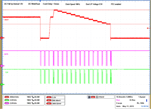
| 1 – Operation only | 4 – 16 VOUT Command up to 1.2 V, | |||
| 2 – Turnoff | 50 mV per step down to 0.6 V | |||
| 3 – Turnon without Margin | 17 – Turnoff | |||
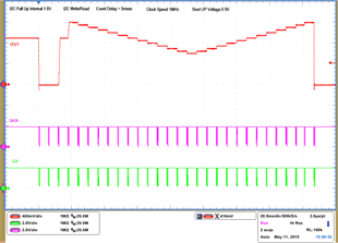
| 1 – Operation only | 4 – 16 VOUT Command up to 1.2 V, 50 mV per step down to 0.6 V | |
| 2 – Turnoff | 17 – 28 Vout Command from 0.6 V to 1.2 V, 50 mV per step | |
| 3 – Turnon without Margin | 29 – Turnoff | |
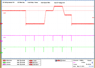
| 1 – Operation only | 4 – VOUT Command up to 1.2 V | |||
| 2 – Turnoff | 5 – VOUT Command down to 0.6 V | |||
| 3 – Turnon without Margin | 6 – Turnoff | |||
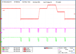
| 1 – Operation only | 4 – VOUT Command up to 1.2 V | |||
| 2 – Turnoff | 5 – VOUT Command down to 0.6 V | |||
| 3 – Turnon without Margin | 6 – Turnoff | |||
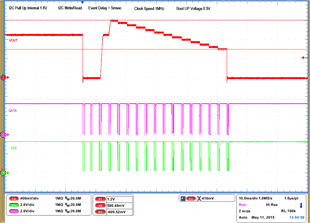
| 1 – Operation only | 4 – 16 VOUT Command up to 1.2 V, | |||
| 2 – Turnoff | 50 mV per step down to 0.6 V | |||
| 3 – Turnon without Margin | 17 – Turnoff | |||
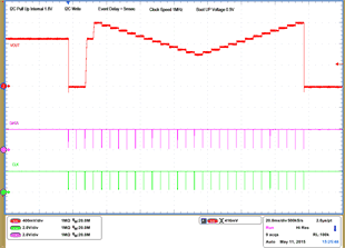
| 1 – Operation only | 4 – 16 VOUT Command up to 1.2 V, | |||
| 2 – Turnoff | 50 mV per step down to 0.6 V | |||
| 3 – Turnon without Margin | 17 – 28 VOUT Command from 0.6 V to 1.2 V, 50 mV per step | |||
| 29 – Turnoff | ||||
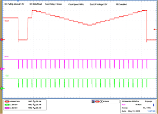
| 1 – Operation only | 4 – 16 Vout Command up to 1.2 V, | |||
| 2 – Turnoff | 50 mV per step down to 0.6 V | |||
| 3 – Turnon without Margin | 17 – 28 Vout Command from 0.6 V to 1.2 V, 50 mV per step | |||
| 29 – Turnoff | ||||