SLVSD29 October 2015 DRV8704
PRODUCTION DATA.
- 1 Features
- 2 Applications
- 3 Description
- 4 Revision History
- 5 Pin Configuration and Functions
- 6 Specifications
-
7 Detailed Description
- 7.1 Overview
- 7.2 Functional Block Diagram
- 7.3 Feature Description
- 7.4 Device Functional Modes
- 7.5
Register Maps
- 7.5.1
Control Registers
- 7.5.1.1 CTRL Register (Address = 0x00h)
- 7.5.1.2 TORQUE Register (Address = 0x01h)
- 7.5.1.3 OFF Register (Address = 0x02h)
- 7.5.1.4 BLANK Register (Address = 0x03h)
- 7.5.1.5 DECAY Register (Address = 0x04h)
- 7.5.1.6 Reserved Register Address = 0x05h
- 7.5.1.7 DRIVE Register Address = 0x06h
- 7.5.1.8 STATUS Register (Address = 0x07h)
- 7.5.1
Control Registers
- 8 Application and Implementation
- 9 Power Supply Recommendations
- 10Layout
- 11Device and Documentation Support
- 12Mechanical, Packaging, and Orderable Information
パッケージ・オプション
メカニカル・データ(パッケージ|ピン)
- DCP|38
サーマルパッド・メカニカル・データ
- DCP|38
発注情報
7.3.4 Decay Modes
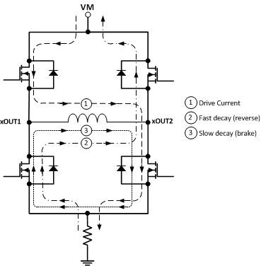
During PWM current chopping, the H-bridge is enabled to drive current through the motor winding until the PWM current chopping threshold is reached. This is shown in the diagram below as case 1. The current flow direction shown indicates positive current flow in the step table below.
Once the chopping current threshold is reached, the H-bridge can operate in two different states, fast decay or slow decay.
In fast decay mode, once the PWM chopping current level has been reached, the H-bridge reverses state to allow winding current to flow in a reverse direction. If the winding current approaches zero, the bridge is disabled to prevent any reverse current flow. Fast decay mode is shown in the diagram below as case 2.
In slow decay mode, winding current is recirculated by enabling both of the low-side FETs in the bridge. This is shown as case 3 in Figure 9.
 Figure 9. Decay Mode Current
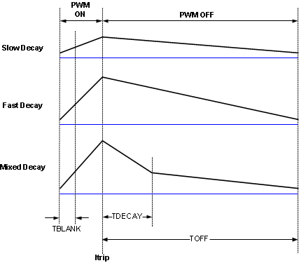
  Figure 10. Decay Mode Comparison
 The DRV8704 supports fast decay and slow decay modes. In addition it supports fixed mixed decay and auto mixed decay modes. Decay mode is selected by the DECMOD bits in the DECAY register.
Mixed decay mode begins as fast decay, but after a programmable period of time (set by the TDECAY bits in the DECAY register) switches to slow decay mode for the remainder of the fixed off time.
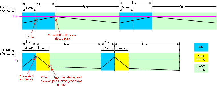
Auto mixed decay mode samples the current level at the end of the blanking time, and if the current is above the Itrip threshold, immediately changes the H-bridge to fast decay. During fast decay, the (negative) current is monitored, and when it falls below the Itrip threshold (and another blanking time has passed), the bridge is switched to slow decay. Once the fixed off time expires, a new cycle is started.
If the bridge is turned on and at the end of tBLANK the current is below the Itrip threshold, the bridge remains on until the current reaches Itrip. Then slow decay is entered for the fixed off time, and a new cycle begins.
Refer to Figure 11.
The upper waveform shows the behavior if I < Itrip at the end of tBLANK. This is a stable, slow decay mode of operation.
The lower waveform shows what happens when I > Itrip at the end of tBLANK. Note that (at slow motor speeds, where back EMF is not significant), the current increase during the ON phase is the same magnitude as the current decrease in fast decay, since both times are controlled by tBLANK, and the rate of change is the same (full VM is applied to the load inductance in both cases, but in opposite directions). In this case, the current will gradually be driven down until the peak current is just hitting Itrip at the end of the blanking time, after which some cycles will be slow decay, and some will be mixed decay.
 Figure 11. Auto Mixed Decay
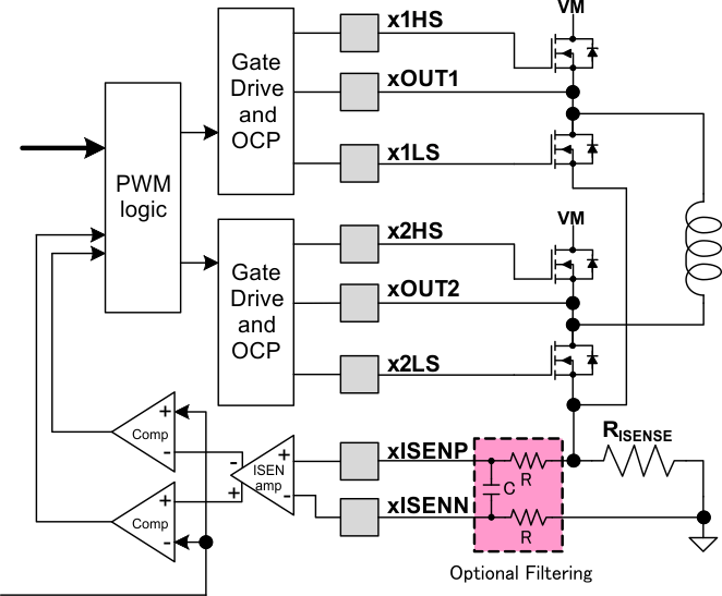
 To accurately detect zero current, an internal offset has been intentionally placed in the zero current detection circuit. If an external filter is placed on the current sense resistor to the xISENN and xISENP pins, symmetry must be maintained. This means that any resistance between the bottom of the RISENSE resistor and xISENN must be matched by the same resistor value (1% tolerance) between the top of the RISENSE resistor and xISENP. Ensure a maximum resistance of 500 Ω. The capacitor value should be chosen such that the RC time constant is between 50 and 60 ns. Any external filtering on these pins is optional and not required for operation.
 Figure 12. Optional Filtering for Sense Amplifiers