SLVSD29 October 2015 DRV8704
PRODUCTION DATA.
- 1 Features
- 2 Applications
- 3 Description
- 4 Revision History
- 5 Pin Configuration and Functions
- 6 Specifications
-
7 Detailed Description
- 7.1 Overview
- 7.2 Functional Block Diagram
- 7.3 Feature Description
- 7.4 Device Functional Modes
- 7.5
Register Maps
- 7.5.1
Control Registers
- 7.5.1.1 CTRL Register (Address = 0x00h)
- 7.5.1.2 TORQUE Register (Address = 0x01h)
- 7.5.1.3 OFF Register (Address = 0x02h)
- 7.5.1.4 BLANK Register (Address = 0x03h)
- 7.5.1.5 DECAY Register (Address = 0x04h)
- 7.5.1.6 Reserved Register Address = 0x05h
- 7.5.1.7 DRIVE Register Address = 0x06h
- 7.5.1.8 STATUS Register (Address = 0x07h)
- 7.5.1
Control Registers
- 8 Application and Implementation
- 9 Power Supply Recommendations
- 10Layout
- 11Device and Documentation Support
- 12Mechanical, Packaging, and Orderable Information
パッケージ・オプション
メカニカル・データ(パッケージ|ピン)
- DCP|38
サーマルパッド・メカニカル・データ
- DCP|38
発注情報
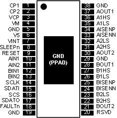
5 Pin Configuration and Functions
DCP Package
38-Pin HTSSOP
Top View

Pin Functions
| PIN (1) | TYPE | DESCRIPTION | ||
|---|---|---|---|---|
| NAME | NO. | |||
| POWER AND GROUND | ||||
| CP1 | 1 | IO | Charge pump flying capacitor | Connect a 0.1-μF X7R capacitor between CP1 and CP2. Voltage rating must be greater than applied VM voltage. |
| CP2 | 2 | IO | Charge pump flying capacitor | |
| GND | 5, 19, 29, 38, PPAD | — | Device ground | All pins must be connected to ground |
| RSVD | 20 | — | Reserved | Leave this pin disconnected |
| V5 | 6 | O | 5-V regulator output | 5-V linear regulator output. Bypass to GND with a 0.1-μF 10-V X7R ceramic capacitor. |
| VCP | 3 | IO | High-side gate drive voltage | Connect a 1-μF 16-V X7R ceramic capacitor to VM |
| VINT | 7 | — | Internal logic supply voltage | Logic supply voltage. Bypass to GND with a 1-μF 6.3-V X7R ceramic capacitor. |
| VM | 4 | — | Motor power supply | Connect to motor supply voltage. Bypass to GND with a 0.1-μF ceramic capacitor plus a 100-μF electrolytic capacitor. |
| CONTROL | ||||
| AIN1 | 10 | I | Bridge A IN1 | Controls bridge A OUT1. Internal pulldown. |
| AIN2 | 11 | I | Bridge A IN2 | Controls bridge A OUT2. Internal pulldown. |
| BIN1 | 12 | I | Bridge B IN1 | Controls bridge B OUT1. Internal pulldown. |
| BIN2 | 13 | I | Bridge B IN2 | Controls bridge B OUT2. Internal pulldown. |
| RESET | 9 | I | Reset input | Active-high reset input initializes all internal logic and disables the H-bridge outputs. Internal pulldown. |
| SLEEPn | 8 | I | Sleep mode input | Logic high to enable device, logic low to enter low-power sleep mode. Internal pulldown. |
| SERIAL INTERFACE | ||||
| SCLK | 14 | I | Serial clock input | Rising edge clocks data into part for write operations. Falling edge clocks data out of part for read operations. Internal pulldown. |
| SCS | 16 | I | Serial chip select input | Active high to enable serial data transfer. Internal pulldown. |
| SDATI | 15 | I | Serial data input | Serial data input from controller. Internal pulldown. |
| SDATO | 17 | O | Serial data output | Serial data output to controller. Open-drain output requires external pull-up. |
| STATUS | ||||
| FAULTn | 18 | OD | Fault | Logic low when in fault condition. Open-drain output requires external pullup. |
| OUTPUT | ||||
| A1HS | 36 | O | Bridge A out 1 HS gate | Bridge A out 1 HS FET gate |
| A1LS | 35 | O | Bridge A out 1 LS gate | Bridge A out 1 LS FET gate |
| A2HS | 31 | O | Bridge A out 2 HS gate | Bridge A out 2 HS FET gate |
| A2LS | 32 | O | Bridge A out 2 LS gate | Bridge A out 2 LS FET gate |
| AISENN | 33 | I | Bridge A Isense – in | Ground at sense resistor for bridge A |
| AISENP | 34 | I | Bridge A Isense + in | Current sense resistor for bridge A |
| AOUT1 | 37 | I | Bridge A output 1 | Output node of bridge A out 1 |
| AOUT2 | 30 | I | Bridge A output 2 | Output node of bridge A out 2 |
| B1HS | 27 | O | Bridge B out 1 HS gate | Bridge B out 1 HS FET gate |
| B1LS | 26 | O | Bridge B out 1 LS gate | Bridge B out 1 LS FET gate |
| B2HS | 22 | O | Bridge B out 2 HS gate | Bridge B out 2 HS FET gate |
| B2LS | 23 | O | Bridge B out 2 LS gate | Bridge B out 2 LS FET gate |
| BISENN | 24 | I | Bridge B Isense – in | Ground at sense resistor for bridge B |
| BISENP | 25 | I | Bridge B Isense + in | Current sense resistor for bridge B |
| BOUT1 | 28 | I | Bridge B output 1 | Output node of bridge B out 1 |
| BOUT2 | 21 | I | Bridge B output 2 | Output node of bridge B out 2 |
(1) Directions: I = Input, O = Output, OZ = Tri-state output, OD = Open-drain output, IO = Input/output