SLWU087E november 2013 – june 2023
- 1
- High Speed Data Converter Pro GUI
- Trademarks
- 1 Introduction
- 2 Software Start up
-
3 User Interface
- 3.1
Toolbar
- 3.1.1 File Options
- 3.1.2 Instrument Options
- 3.1.3 Data Capture Option
- 3.1.4
Test Options
- 3.1.4.1 Notch Frequency Bins
- 3.1.4.2 2 Channel Display and Cursor Lock
- 3.1.4.3 Analysis Window Markers
- 3.1.4.4 X-Scale in Time
- 3.1.4.5 Y-Scale in Voltage
- 3.1.4.6 Other Frequency Options
- 3.1.4.7 NSD Marker
- 3.1.4.8 Phase Plot
- 3.1.4.9 Phase in Degree
- 3.1.4.10 Histogram
- 3.1.4.11 Disable User Popups
- 3.1.4.12 HSDC Pro Lite Version
- 3.1.5 Help
- 3.2 Status Windows
- 3.3 Mode Selection
- 3.4 Device Selection
- 3.5 Skip Configuration
- 3.6 Capture Button (ADC Mode Only)
- 3.7 Test Selection (ADC Mode only)
- 3.8 DAC Display Panel (DAC Mode only)
- 3.9 I/Q Multi-Tone Generator
- 3.1
Toolbar
- 4 ADC Data Capture Software Operation
- 5 TSW1400 Pattern Generator Operation
- 6 TSW14J58 Functional Description
- 7 TSW14J57 Functional Description
- 8 TSW14J56 Functional Description
- 9 TSW14J50 Functional Description
- 10TSW14J10 Functional Description
- A Signal Processing in High Speed Data Converter Pro
- B History Notes
- C Revision History
5.4 Testing a TSW1400 EVM with a DAC5688EVM (CMOS Interface)
This section describes the operation when testing with a DAC5688 EVM that has a CMOS input interface.
- Power down the TSW1400 if the DAC5688 EVM is not installed.
J1 pin 1 of the TSW1400 connector plugs into J2 pin 1 on the DAC5688 EVM
- Provide unpowered +3.3 VDC connections to J15 and return to J16 of the DAC5688 EVM.
- Provide unpowered +1.8 VDC connections to J13 and return to J14 of the DAC5688 EVM.
- Provide a USB cable between the DAC5688 EVM and a host PC.
- Provide an external sinewave source at 491.52 MHz with a 1-Vrms, 0-V offset to SMA J20 (EXT_VCXO) of the DAC5688 EVM.
- Connect a SMA cable from OUTCLK3 connector (J17) of the DAC5688 EVM to CMOS_CLK (J7) of the TSW1400 EVM.
- Power up the TSW1400 followed by the DAC EVM.
- Load and start up the DAC5688 EVM GUI as described in the DAC5688EVM User’s Guide. The software and User’s Guide can be found at http://www.ti.com/tool/dac5688evm.
- Start up the HSDC Pro GUI as described in the Software Start Up section.
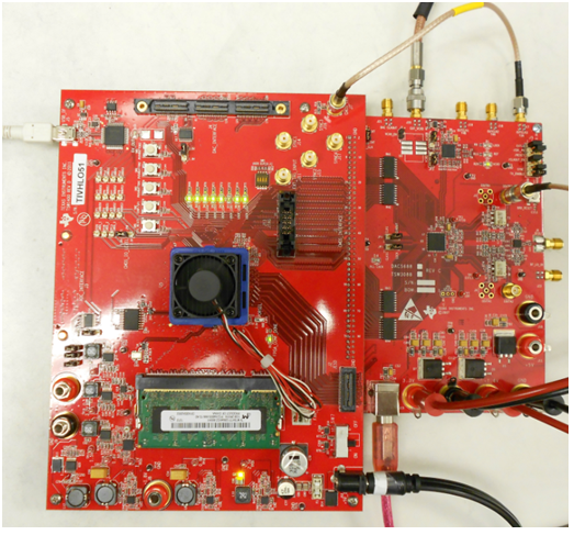
- The TSW1400 EVM connected to the CMOS connectors of the DAC5688 EVM is shown in Figure 5-5
 Figure 5-5 TSW1400EVM Interfacing to the CMOS Connectors of a DAC5688EVM
Using the DAC5688 EVM GUI, load the EVM with the test file called “example”. This can be found at C:\Program Files (x86)\Texas Instruments\DAC5688\DAC5688 Configuration Files. This sets up the DAC5688 to receive a WCDMA test pattern from the TSW1400 with a data rate of 122.88 MHz. CLK2 of DAC5688 operates at 491.52 MHz and the DAC interpolation is set to 4x, requiring the input data rate to be at 122.88 MHz.
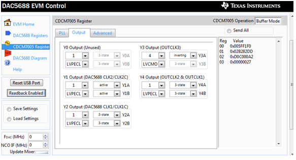
In the DAC5688 GUI, go to the CDCM7005 tab and set the Y3 Output (OUTCLK3) to divide by 4, LVCMOS, and inverting per Figure 5-6.
 Figure 5-6 CDCM7005 Tab on DAC5688 GUI
This generates an inverted 122.88-MHz clock used by the TSW1400 to generate the CMOS test pattern.
The CMOS data rate for the TSW1400 EVM should never exceed 250 MHz. This rate is set by the CMOS_CLOCK input provide to J7. When operating at frequencies near this limit, the user may need to adjust the delay of this signal to meet the timing specs of the DAC under test.
On the DAC5688 EVM, there is an option to use a spare output of the CDCM7005 clock generator as a clock source. In this example, the OUTCLK3 of the CDCM7005 is inverted for optimized setup and hold time. Another way to adjust the delay is to use different cable lengths for this clock source.
If opening the HSDC Pro GUI for the first time, when setting up for pattern generator mode, make sure “DAC” in the top right side of the GUI is selected. This targets the EVM for this test example. In the “Select DAC” button of the GUI, click on the drop down arrow and select “cmos”. This firmware is used by most High Speed CMOS DAC EVM’s.
Click on “Yes” when asked “Do you want to update the firmware for DAC”. The firmware setup is loaded during this process, which takes approximately 20 seconds. After the firmware load has completed, the LED’s labeled USER_LED (0–7) will now turn on except for USER_LED 5. USER_LED 3 is used to indicate the status of a second PLL, and USER_LED 5 indicates if there is a FIFO overflow (error) of the transmit data.
If the TSW1400 is not receiving a valid clock from the DAC EVM, USER_LED3 and USER_LED4 are off.
For this test, at the top of the GUI, set the following parameters:
- Scaling factor to 1
- Preamble to 0
- Data Rate – 122.88M (MSPS)
- DAC Option – 2’s Complement
- Active Channel – Channel 1
- Click on the button labeled “Load External Pattern File”.
- Select “WCDMA_TM1_complexIF30MHz_Fdata122.88MHz_1000.csv”.
- Click on “Send”.
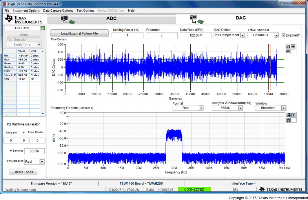
The display panel of the GUI is updated, showing the test data that is transmitted to the DAC EVM in both codes and frequency domain as shown in Figure 5-7.
 Figure 5-7 GUI After Test File Loaded
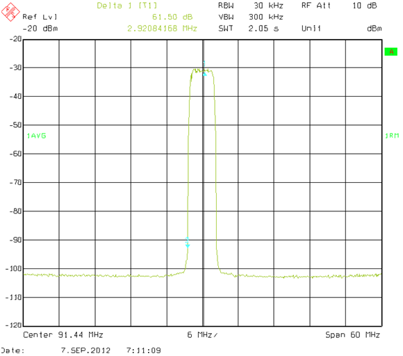
If the DAC5688 EVM is configured for IF output, connect a spectrum analyzer to either SMA J4 (IOUTB2) or J9 (IOUTA2) of the EVM. The DAC example file has a NCO setting of 61.44 MHz and the test pattern IF is centered at 30 MHz. The signal should be a single carrier centered around 91.44 MHz, as shown in Figure 5-8.
The DAC5688 EVM has the default setup as RF output. The modulator output location will be at the LO frequency plus 91.44 MHz. For details about IF and RF output configuration settings, see section 4.7 of the DAC5688 EVM User’s Guide (SLAU241).
 Figure 5-8 DAC5688 IF Output