SLWU087E november   2013  – june 2023


  1.   1
  2.   High Speed Data Converter Pro GUI
  3.   Trademarks
  4. Introduction
  5. Software Start up
    1. 2.1 Installation Instructions
    2. 2.2 USB Interface and Drivers
    3. 2.3 Device ini Files
  6. User Interface
    1. 3.1 Toolbar
      1. 3.1.1 File Options
        1. 3.1.1.1 User Profiles
        2. 3.1.1.2 Resize Window
      2. 3.1.2 Instrument Options
        1. 3.1.2.1 TSW14J56 and High Speed Data Converter (HSDC) Pro Eye Quality Analysis
        2. 3.1.2.2 IO Delay
        3. 3.1.2.3 JESD204B Error Injection
        4. 3.1.2.4 FPGA Registers Write Read
      3. 3.1.3 Data Capture Option
        1. 3.1.3.1 Capture Option
        2. 3.1.3.2 Trigger Option
        3. 3.1.3.3 Using Multiple TSW14xxx and ADC EVM’s for Simultaneous Capture using Trigger Option
          1. 3.1.3.3.1 Hardware Setup
          2. 3.1.3.3.2 Setting up the Slave Board
          3. 3.1.3.3.3 Setting up the Master Board
          4. 3.1.3.3.4 Read Captured Memory from the Slave Board
      4. 3.1.4 Test Options
        1. 3.1.4.1  Notch Frequency Bins
        2. 3.1.4.2  2 Channel Display and Cursor Lock
        3. 3.1.4.3  Analysis Window Markers
        4. 3.1.4.4  X-Scale in Time
        5. 3.1.4.5  Y-Scale in Voltage
        6. 3.1.4.6  Other Frequency Options
        7. 3.1.4.7  NSD Marker
        8. 3.1.4.8  Phase Plot
        9. 3.1.4.9  Phase in Degree
        10. 3.1.4.10 Histogram
        11. 3.1.4.11 Disable User Popups
        12. 3.1.4.12 HSDC Pro Lite Version
      5. 3.1.5 Help
    2. 3.2 Status Windows
    3. 3.3 Mode Selection
    4. 3.4 Device Selection
    5. 3.5 Skip Configuration
    6. 3.6 Capture Button (ADC Mode Only)
    7. 3.7 Test Selection (ADC Mode only)
      1. 3.7.1 Single Tone FFT
        1. 3.7.1.1 Parameter Controls
        2. 3.7.1.2 ADC Captured Data Display Pane
        3. 3.7.1.3 FFT Power Spectrum
        4. 3.7.1.4 Overlay Unwrap Waveform
        5. 3.7.1.5 Single Tone FFT Statistics
      2. 3.7.2 Multi Channel Display
      3. 3.7.3 Unit Selection
      4. 3.7.4 Time Domain
      5. 3.7.5 Two Tone
      6. 3.7.6 Channel Power
    8. 3.8 DAC Display Panel (DAC Mode only)
      1. 3.8.1 Send Button (DAC Mode Only)
      2. 3.8.2 Load File to Transfer into TSW14xxx Button
      3. 3.8.3 Parameter Controls
    9. 3.9 I/Q Multi-Tone Generator
  7. ADC Data Capture Software Operation
    1. 4.1 Testing a TSW1400 EVM with an ADS5281 EVM
    2. 4.2 Testing a TSW1400EVM with an ADS62P49EVM (CMOS Interface)
  8. TSW1400 Pattern Generator Operation
    1. 5.1 Testing a TSW1400 EVM with a DAC3152 EVM
    2. 5.2 Loading DAC Firmware
    3. 5.3 Configuring TSW1400 for Pattern Generation
    4. 5.4 Testing a TSW1400 EVM with a DAC5688EVM (CMOS Interface)
  9. TSW14J58 Functional Description
    1. 6.1 Testing the TSW14J58 EVM with an ADC12DJ3200 EVM
  10. TSW14J57 Functional Description
    1. 7.1 Testing the TSW14J57 EVM with an ADC34J45 EVM
  11. TSW14J56 Functional Description
    1. 8.1 Testing the TSW14J56 EVM with an ADC34J45 EVM
  12. TSW14J50 Functional Description
    1. 9.1 Device Selection
  13. 10TSW14J10 Functional Description
    1. 10.1 DAC and ADC GUI Configuration File Changes When Using a Xilinx Development Platform
    2. 10.2 DAC38J84EVM GUI Setup Example
  14.   A Signal Processing in High Speed Data Converter Pro
    1.     A.1 Introduction
    2.     A.2 FFT Calculation from Time Domain Data
      1.      A.2.1 FFT Window Correction Factor
    3.     A.3 FFT Filtering
    4.     A.4 Single Tone Parameters
      1.      A.4.1 Number of Neighboring Bins for each FFT Window
    5.     A.5 Fundamental Power
      1.      A.5.1 Harmonic Distortions
      2.      A.5.2 SNR
      3.      A.5.3 SFDR
      4.      A.5.4 THD
      5.      A.5.5 SINAD
      6.      A.5.6 ENOB
      7.      A.5.7 Next Spur
    6.     A.6 Two Tone Parameters
    7.     A.7 Average FFT Calculation
    8.     A.8 NSD Calculation
  15.   B History Notes
  16.   C Revision History

IO Delay

The “IO Delay” Calibration process sweeps the IO Delay tap values across a lane and get the tap values where there are no bit errors. Selecting the IO Delay opens the window shown in Figure 3-6. This allows the user to calibrate the lane wise delay adjustments.
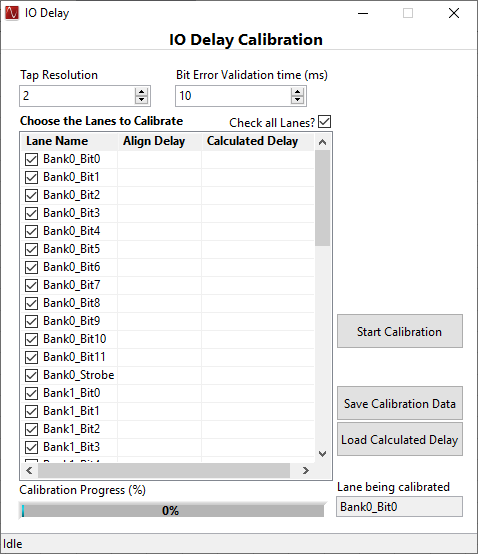
GUID-20210414-CA0I-SFJB-5LMM-SKBBCZ3KM4K5-low.png Figure 3-6 IO Delay Calibration

Calibration is done sequentially for the selected lanes, one after the other. The “Tap Resolution” denotes the minimum step size with which the tap values are swept across IO Delay tap values. “Bit Error Validation time (ms)” specifies the time delay to wait before checking if the Error Bit is true/false while sweeping across the IO Delay tap vales. “Check all Lanes?” can be used to check/uncheck all the lanes. After selecting the required lanes to calibrate, click on the “Start Calibration Data” button to run the calibration on the selected lanes one after the other. Once calibration has been started (“Start Calibration” then turns into “Stop Calibration”), it can be stopped anytime using “Stop Calibration” button. After the calibration completes, the calibrated data can be saved by clicking on “Save Calibration Data” and entering the target file location. Click on “Load Calculated Delay” and load the previously saved file with Calibration data, this action derives the “Calculated Delay” for all the selected/calibrated lanes and the same calculated delay gets loaded to the FW. This completes the IO Delay Calibration. After the IO Delay Calibration steps are done, data capture can be done from HSDC Pro as usual.

Note: Currently the IO Delay option is supported only in the TSW14DL3200 EVM board. Do not close the IO Delay window when the calibration is running. If closed when the calibration is running, restart HSDC Pro. Before doing the calibration, make sure that the FW has been downloaded and no capture/calibration has been done after the FW download.