SLWU087E november 2013 – june 2023
- 1
- High Speed Data Converter Pro GUI
- Trademarks
- 1 Introduction
- 2 Software Start up
-
3 User Interface
- 3.1
Toolbar
- 3.1.1 File Options
- 3.1.2 Instrument Options
- 3.1.3 Data Capture Option
- 3.1.4
Test Options
- 3.1.4.1 Notch Frequency Bins
- 3.1.4.2 2 Channel Display and Cursor Lock
- 3.1.4.3 Analysis Window Markers
- 3.1.4.4 X-Scale in Time
- 3.1.4.5 Y-Scale in Voltage
- 3.1.4.6 Other Frequency Options
- 3.1.4.7 NSD Marker
- 3.1.4.8 Phase Plot
- 3.1.4.9 Phase in Degree
- 3.1.4.10 Histogram
- 3.1.4.11 Disable User Popups
- 3.1.4.12 HSDC Pro Lite Version
- 3.1.5 Help
- 3.2 Status Windows
- 3.3 Mode Selection
- 3.4 Device Selection
- 3.5 Skip Configuration
- 3.6 Capture Button (ADC Mode Only)
- 3.7 Test Selection (ADC Mode only)
- 3.8 DAC Display Panel (DAC Mode only)
- 3.9 I/Q Multi-Tone Generator
- 3.1
Toolbar
- 4 ADC Data Capture Software Operation
- 5 TSW1400 Pattern Generator Operation
- 6 TSW14J58 Functional Description
- 7 TSW14J57 Functional Description
- 8 TSW14J56 Functional Description
- 9 TSW14J50 Functional Description
- 10TSW14J10 Functional Description
- A Signal Processing in High Speed Data Converter Pro
- B History Notes
- C Revision History
7.1 Testing the TSW14J57 EVM with an ADC34J45 EVM
This section describes the operation when testing with an ADC34J45 EVM that has a JESD204B output interface.
- Power down the TSW14J57 if an ADC EVM is not installed.
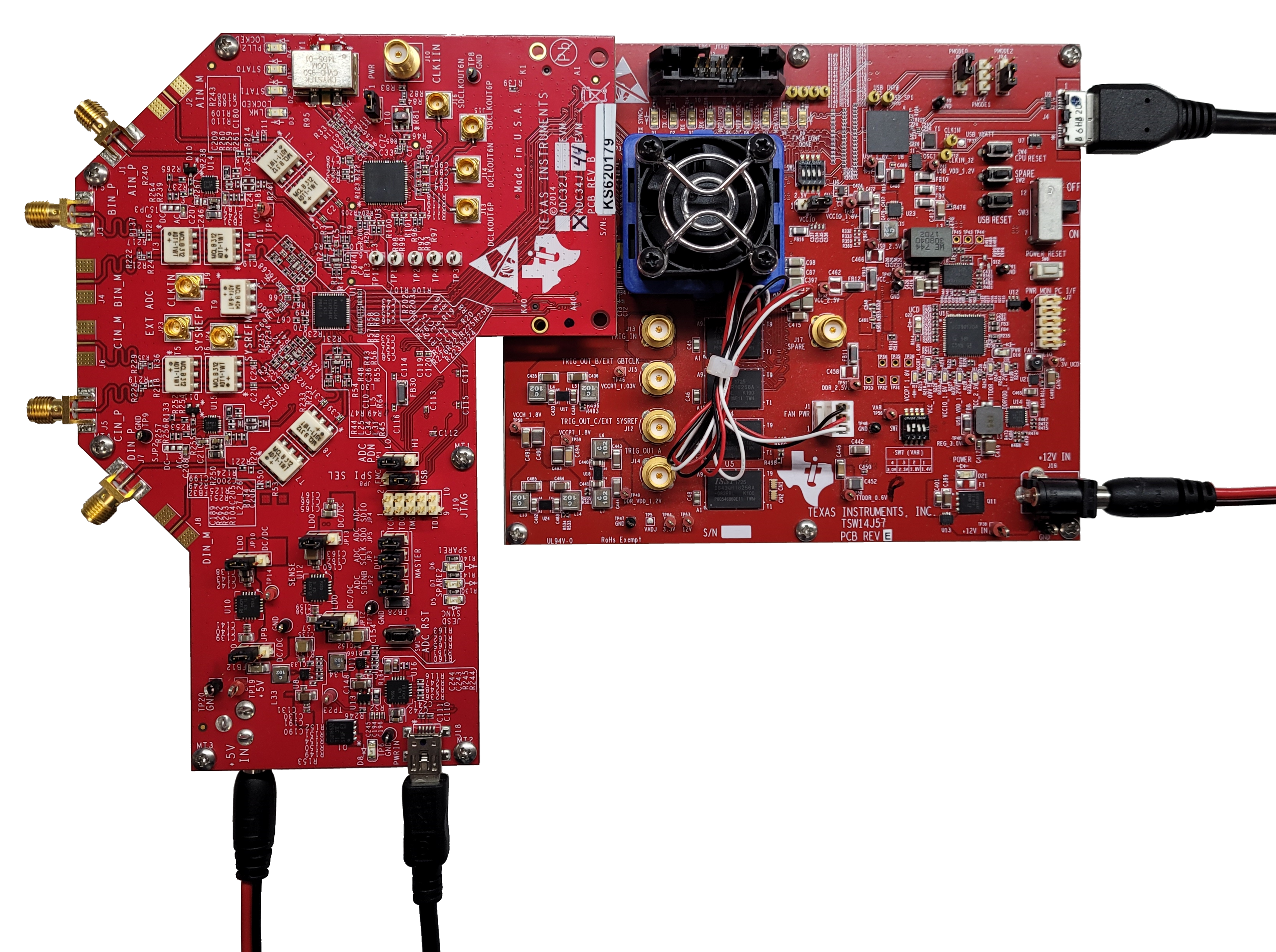
- Connect J17 of the ADC34J45 EVM to connector J2 of the TSW14J57.
- Provide +5 VDC connection to J20 of the ADC34J45 EVM and +12 VDC connection to J16 of the TSW14J57 EVM.
- Connect a USB 3.0 cable to J4 of the TSW14J57 EVM and a USB 2.0 cable to J18 of the ADC34J45 EVM.
- Power up the TSW14J57 followed by the ADC EVM.
- The TSW14J57 EVM connected to an ADC34J45 EVM is shown in Figure 7-6
 Figure 7-2 TSW14J57 EVM connected to an ADC34J45 EVM
Single Tone FFT Test
- The evaluation of the ADC34J45 EVM requires programming the LMK04828 clock source with the correct PLL settings to provide a 160 Msps clock.
- Open the ADC3000 GUI, and connect to the ADC34J45 EVM
- Go to the Low Level tab and click Load Config
- Browse and find the ADC3xJxx_160MSPS_Operation_LMK_Setting.cfg
- Check that the PLL2 LED D4 is lit on the ADC34J45 EVM – this indicates that the PLL is programmed properly and the correct clocks are being generated
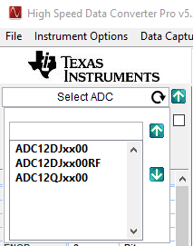
- Start the HSDC Pro GUI program. When the program starts, select the ADC tab and then select ADC34J4x_LMF_442 device in the Select ADC drop-down menu as seen in Figure 7-7.
 Figure 7-3 Select ADC34Jxx in the HSDC Pro GUI Program
 - When prompted by Load ADC Firmware?, select YES
- Select Single Tone FFT Test under Test Selection
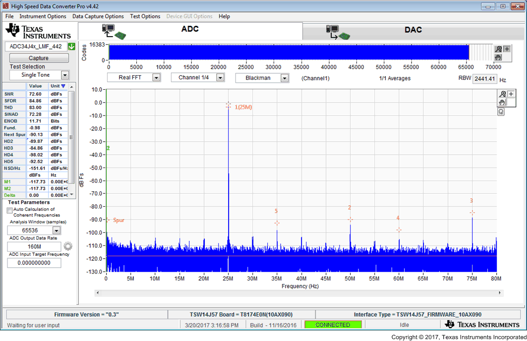
- Select the number of sample points (and resulting number of FFT bins) to be used. The example shown in Figure 7-8 has 65536 samples.
- Enter the ADC34J45 sampling rate. The example shown in Figure 7-8 has the sample rate set at 160 Msps
- Enter the input frequency desired. The example shown in Figure 7-8 has the filtered input frequency set at 25 MHz and approximately –1 dBFs on the HSDC Pro FFT plot
- Select channel 1, 2, 3, 4 depending on the channel to which the signal generator is connected
- Press the Capture button on the HSDC Pro GUI
- Observe an FFT result similar to that of Figure 7-8
 Figure 7-4 ADC34J45 Operating in 14-Bit Mode at 160 Msps with 25-MHz Input Signal
If the basic capture at this point is correct, then the front panel options of the ADC3000 SPI GUI and the front panel options of the High Speed Data Converter Pro GUI may be varied as desired to test out different device SPI options