SLWU087E november 2013 – june 2023
- 1
- High Speed Data Converter Pro GUI
- Trademarks
- 1 Introduction
- 2 Software Start up
-
3 User Interface
- 3.1
Toolbar
- 3.1.1 File Options
- 3.1.2 Instrument Options
- 3.1.3 Data Capture Option
- 3.1.4
Test Options
- 3.1.4.1 Notch Frequency Bins
- 3.1.4.2 2 Channel Display and Cursor Lock
- 3.1.4.3 Analysis Window Markers
- 3.1.4.4 X-Scale in Time
- 3.1.4.5 Y-Scale in Voltage
- 3.1.4.6 Other Frequency Options
- 3.1.4.7 NSD Marker
- 3.1.4.8 Phase Plot
- 3.1.4.9 Phase in Degree
- 3.1.4.10 Histogram
- 3.1.4.11 Disable User Popups
- 3.1.4.12 HSDC Pro Lite Version
- 3.1.5 Help
- 3.2 Status Windows
- 3.3 Mode Selection
- 3.4 Device Selection
- 3.5 Skip Configuration
- 3.6 Capture Button (ADC Mode Only)
- 3.7 Test Selection (ADC Mode only)
- 3.8 DAC Display Panel (DAC Mode only)
- 3.9 I/Q Multi-Tone Generator
- 3.1
Toolbar
- 4 ADC Data Capture Software Operation
- 5 TSW1400 Pattern Generator Operation
- 6 TSW14J58 Functional Description
- 7 TSW14J57 Functional Description
- 8 TSW14J56 Functional Description
- 9 TSW14J50 Functional Description
- 10TSW14J10 Functional Description
- A Signal Processing in High Speed Data Converter Pro
- B History Notes
- C Revision History
7 TSW14J57 Functional Description
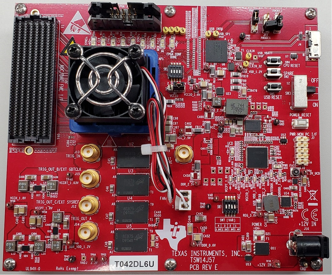
The TI TSW14J57 EVM is a pattern generator and data capture card with a JESD204B serial interface. The TSW14J57 has an FMC+ connector that can be used to evaluate the performance of the TI JESD204B device family ADCs and DACs (see Figure 7-1). For an ADC, the high speed serial data is captured and de-serialized and formatted by an Intel PSG®Arria® 10 FPGA, then stored in an onboard DDR4 SDRAM, allowing the TSW14J57 to store up to 1G of 16-bit samples. It also supports lane speeds from 2 Gbps to 15 Gbps, from 1 to 16 lanes with one firmware build. Together with the accompanying HSDC Pro GUI, it is a complete system that captures and evaluates data samples from ADC EVMs and generates and sends desired test patterns to DAC EVMs.
To acquire data on a host PC, the FPGA reads the data from memory and transmits it on SPI. An onboard high-speed USB-to-SPI converter bridges the FPGA SPI interface to the host PC and GUI.
In Pattern Generator Mode, the TSW14J57 generates desired test patterns for DAC EVMs under test. These patterns are sent from the host PC over the USB interface to the TSW14J57. The FPGA stores the data received into the board DDR4 memory module. The data from the memory is then read by the FPGA and transmitted to a DAC EVM across the JESD204B interface connector.
In the Instrument Options tab of the GUI, the option called "Dynamic Configuration" allows the user to change certain JESD204B parameters without loading new firmware into the FPGA. The ini files load default values for these parameters based on what ADC or DAC is selected and what mode of operation is chosen. For the most part, users should not have to change these values in this tab. If any values are changed, the default values of the ini file will be overwritten. Any changes will effect the operation of the JESD204B interface and will have to be made at both the receiver and transmit side of the interface.
 Figure 7-1 TSW14J57 EVM