SLOA277B january 2019 – july 2023 LM124 , LM124-N , LM124A , LM158 , LM158-N , LM158A , LM224 , LM224-N , LM224A , LM258 , LM258-N , LM258A , LM2902 , LM2902-N , LM2902-Q1 , LM2902K , LM2902KAV , LM2904 , LM2904-N , LM2904-Q1 , LM2904B , LM2904B-Q1 , LM2904BA , LM321 , LM324 , LM324-N , LM324A , LM358 , LM358-N , LM358A , LM358B , LM358BA , TS321 , TS321-Q1
4.2 Slew Rate Variability
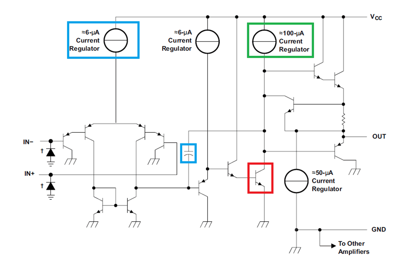
It is best to allow for some margin between the application's slew rate requirement and the typical slew rate of the device used. Normal process variance affects internal bias currents and capacitor oxide thickness, which are two factors that determine slew rate. These components are highlighted in blue in Figure 4-1. There may also be a slight difference between the positive and negative slew rates. The reason for this difference is simple: the transistor in the red box in Figure 4-1 has no turn off drive. The NPN transistor driving the red box transistor can only source current to turn on, but cannot sink current to turn off. The base to collector capacitance of the transistor in the red box in this device family varies among the dies in production. The beta of the NPN transistor is also a factor in determining slew rate. If the natural turn off slew rate of the red boxed transistor
is slower than the slew rate set by the bias and compensation capacitor
then the positive slew rate is reduced while the negative slew rate is not affected. Hence, the positive slew rate can be slower than the negative slew rate. LM358B, LM2904B, LM324B, and LM2902B have a discharge path for the base of the red boxed transistor. Therefore, the slew rate is not affected by this highlighted transistor.
 Figure 4-1 Schematic With the Following Slew Rate Components
Highlighted: Tail Current (Blue), Compensation
Capacitor (Blue), Collector Current (Green),
Collector to Base Capacitance (Red)
Figure 4-1 Schematic With the Following Slew Rate Components
Highlighted: Tail Current (Blue), Compensation
Capacitor (Blue), Collector Current (Green),
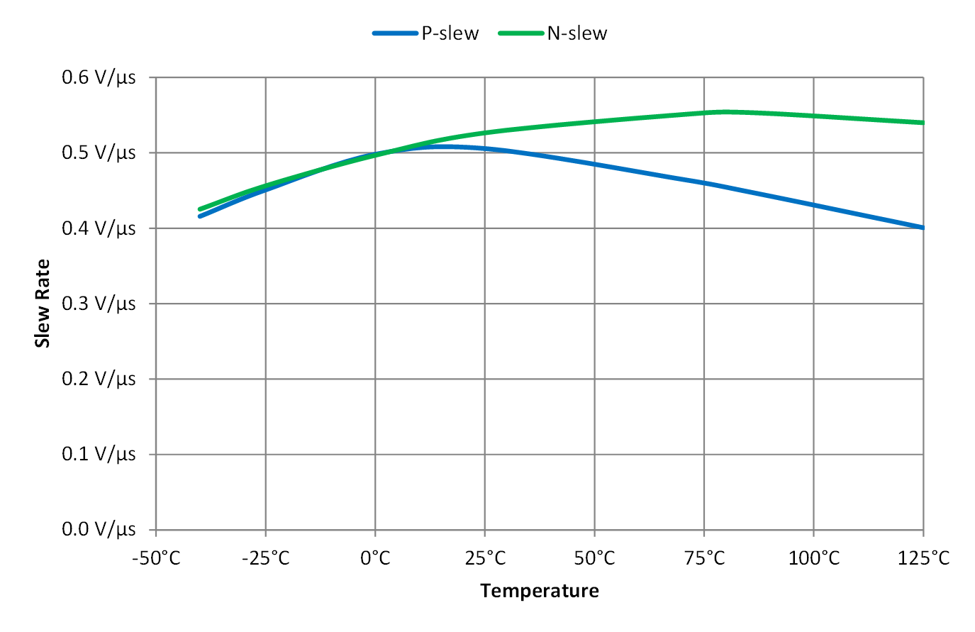
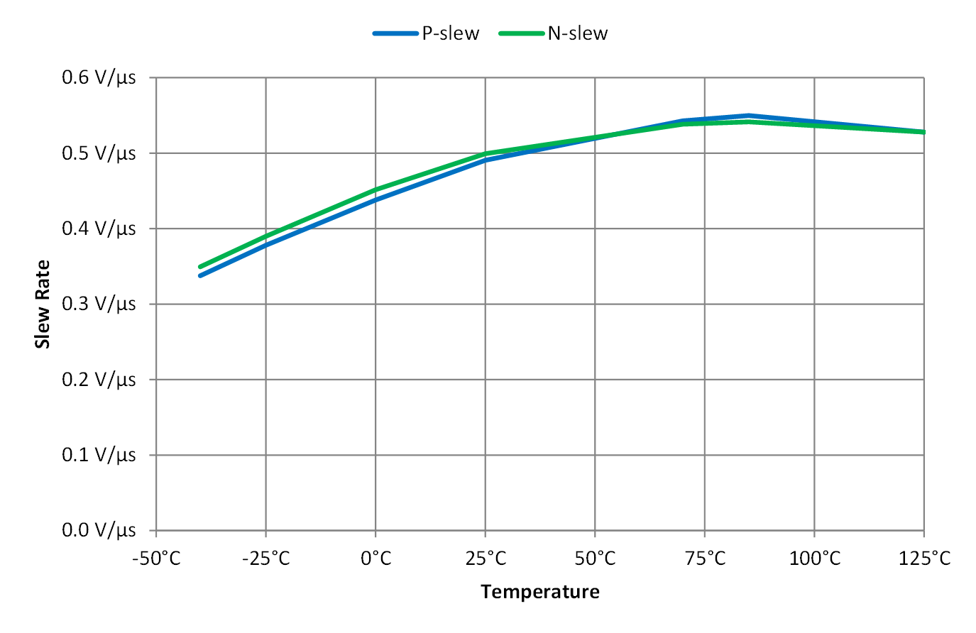
Collector to Base Capacitance (Red)Only the commercial grade quad op amp with the widest input offset specification has a die with enough base-collector capacitance to typically demonstrate variation in high temperature slew rates. Slew rate differing in all other device variants will be a rare occurrence. The key point is not to depend on matching slew rate. Fortunately, few circuits actually require matching slew rate. For reference, the slew rate curves of two common devices are shown below with the commercial grade in Figure 4-2 and the automotive grade in Figure 4-3. Note that the other die designs typically have matching positive and negative slew rates. A small percentage of samples may exhibit some differences at high temperature.
 Figure 4-2 Plot Showing Slew Rate vs Temperature for
LM2902DR
 Figure 4-3 Slew Rate vs Temperature for LM2902QDRQ1