SLOA277B january 2019 – july 2023 LM124 , LM124-N , LM124A , LM158 , LM158-N , LM158A , LM224 , LM224-N , LM224A , LM258 , LM258-N , LM258A , LM2902 , LM2902-N , LM2902-Q1 , LM2902K , LM2902KAV , LM2904 , LM2904-N , LM2904-Q1 , LM2904B , LM2904B-Q1 , LM2904BA , LM321 , LM324 , LM324-N , LM324A , LM358 , LM358-N , LM358A , LM358B , LM358BA , TS321 , TS321-Q1
7.2 Unused Amplifier Connections
Occasionally applications will not need all the amplifiers in a dual or quad package. The unused op amp should be connected in a way that is safe for the unused amplifier and doesn’t affect the used amplifiers. The best connection method puts the op amp into the normal linear operation range and no inputs are connected directly to low impedance nodes. The output of the op amp is not a low impedance node. The output by itself cannot provide a harmful voltage and/or current to the input. Therefore, no series resistor is needed between the input and output pins. Figure 7-1 shows preferred connections for unused amplifiers.
 Figure 7-1 Best Connections Practices for
Single and Dual Supplies
Figure 7-1 Best Connections Practices for
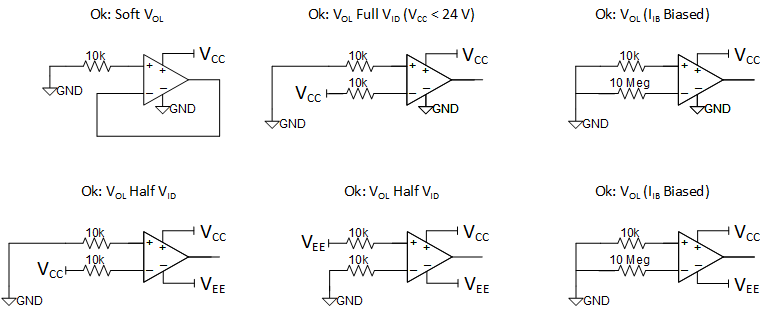
Single and Dual SuppliesAlternatively, the device may be connected in certain, non-linear VOH or VOL configurations, as shown in Figure 7-2. VOL is preferred over VOH because that provides a small reduction in supply current, ICC. LM358B and LM2904B have slightly lower ICC in the VOH configuration. A soft VOL configuration is sometimes linear if VIO is more positive than 1 mV, but it usually creates a non-linear VOL state. Increasing the input resistor to 10 MΩ would ensure linear operation as the input bias current would raise the non-inverting input voltage beyond the input offset voltage range. "VOL Full VID" is better suited for lower voltage applications as there is no reason to apply a large input voltage difference even though the op amp allows it. The "VOL (IIB Biased)" method uses the input bias current to raise the voltage on the inverting input. If used, place the 10-MΩ resistor close to the inverting input pin to reduce noise pickup. No inputs may be connected directly to low impedance nodes such as ground, VCC or VEE. VOH alternatives are also acceptable; just swap the input pins. The "soft VOL" connection cannot be input swapped.
 Figure 7-2 Acceptable Connection Practices for Single and Dual Supplies
The next set of connections in Figure 7-3 is not recommended, but these configurations are not considered harmful methods of terminating unused channels. The VOH alternatives that swap the inputs are also not recommended methods of terminating unused channels.
 Figure 7-3 Less Than Acceptable
Connection Practices for Single and Dual Supplies
Figure 7-3 Less Than Acceptable
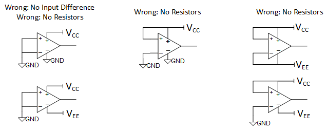
Connection Practices for Single and Dual SuppliesThe last set of connections, seen in Figure 7-4, demonstrates improper setups that could cause output noise chatter or device damage if the GND pin were to ever become positive relative to the input pin.
 Figure 7-4 Potentially Harmful Connection Practices for Single and Dual Supplies