SLOA277B january 2019 – july 2023 LM124 , LM124-N , LM124A , LM158 , LM158-N , LM158A , LM224 , LM224-N , LM224A , LM258 , LM258-N , LM258A , LM2902 , LM2902-N , LM2902-Q1 , LM2902K , LM2902KAV , LM2904 , LM2904-N , LM2904-Q1 , LM2904B , LM2904B-Q1 , LM2904BA , LM321 , LM324 , LM324-N , LM324A , LM358 , LM358-N , LM358A , LM358B , LM358BA , TS321 , TS321-Q1
4.3 Output Crossover Time Delay
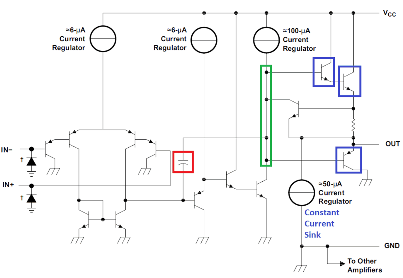
This op amp family does not provide any static bias for any of the output transistors (Class B type) highlighted in the blue boxes in Figure 4-4. Most other op amp designs provide a small static bias to the output transistors (Class AB type) to make output current transitions seamless. The advantage of having no static bias is allowing the ‘Constant Current Sink’ driver to pull the output close to the negative supply voltage. The disadvantage of having no static bias is a time delay when switching between the output source and sink drivers.
 Figure 4-4 Schematic with the Following
Time Delay Components Highlighted: Shared Input Node (Green), Compensation
Capacitor (Red), and Output Transistors (Blue)
Figure 4-4 Schematic with the Following
Time Delay Components Highlighted: Shared Input Node (Green), Compensation
Capacitor (Red), and Output Transistors (Blue)The op amp’s Darlington NPN driver and PNP emitter follower output transistors share an input signal highlighted in the green box. The compensation capacitor is also connected to this common node. Therefore, the slew rate of the green node is the same as the output’s slew rate, which can be found on the data sheet as a typical value. When the op amp needs to change between the Darlington NPN and PNP emitter follower drivers, there is a time delay of approximately
Depending on the application, this delay may or may not be significant. The maximum application frequency and load current range are relevant factors in determining whether or not the time delay will be significant.
Two test circuits, shown in Figure 4-5 and Figure 4-7, are specifically designed to maximize the visual effect of the crossover time delay. In many applications, the crossover time does not cause any issues. However, extra care should be taken when there are high frequency signals, fast rise or fall times, or when distortion must be minimized. Output pull down or pull up resistors can be added to keep either the output source or sink driver continually active, thereby preventing time delays.