SBAS999A June   2019  – January 2021 ADS125H01

PRODUCTION DATA  

  1. Features
  2. Applications
  3. Description
  4. Revision History
  5. Device Comparison Table
  6. Pin Configuration and Functions
  7. Specifications
    1. 7.1 Absolute Maximum Ratings
    2. 7.2 ESD Ratings
    3. 7.3 Recommended Operating Conditions
    4. 7.4 Thermal Information
    5. 7.5 Electrical Characteristics
    6. 7.6 Timing Requirements
    7. 7.7 Switching Characteristics
    8. 7.8 Timing Diagrams
    9. 7.9 Typical Characteristics
  8. Parameter Measurement Information
    1. 8.1 Noise Performance
  9. Detailed Description
    1. 9.1 Overview
    2. 9.2 Functional Block Diagram
    3. 9.3 Feature Description
      1. 9.3.1 Input Voltage Range
      2. 9.3.2 Analog Inputs (AINP, AINN)
        1. 9.3.2.1 ESD Diodes
        2. 9.3.2.2 Input Switch
      3. 9.3.3 Programmable Gain Amplifier (PGA)
        1. 9.3.3.1 PGA Operating Range
        2. 9.3.3.2 PGA Monitors
      4. 9.3.4 Reference Voltage
        1. 9.3.4.1 Reference Monitor
      5. 9.3.5 ADC Modulator
      6. 9.3.6 Digital Filter
        1. 9.3.6.1 Sinc Filter Mode
          1. 9.3.6.1.1 Sinc Filter Frequency Response
        2. 9.3.6.2 FIR Filter
        3. 9.3.6.3 50-Hz and 60-Hz Normal-Mode Rejection
    4. 9.4 Device Functional Modes
      1. 9.4.1 Conversion Control
        1. 9.4.1.1 Continuous-Conversion Mode
        2. 9.4.1.2 Pulse-Conversion Mode
        3. 9.4.1.3 Conversion Latency
        4. 9.4.1.4 Start-Conversion Delay
      2. 9.4.2 Clock Mode
      3. 9.4.3 Reset
        1. 9.4.3.1 Power-On Reset
        2. 9.4.3.2 Reset by RESETPin
        3. 9.4.3.3 Reset by Command
      4. 9.4.4 Calibration
        1. 9.4.4.1 Offset and Full-Scale Calibration
          1. 9.4.4.1.1 Offset Calibration Registers
          2. 9.4.4.1.2 Full-Scale Calibration Registers
        2. 9.4.4.2 Offset Calibration Command (OFSCAL)
        3. 9.4.4.3 Full-Scale Calibration Command (GANCAL)
        4. 9.4.4.4 Calibration Command Procedure
        5. 9.4.4.5 User Calibration Procedure
    5. 9.5 Programming
      1. 9.5.1 Serial Interface
        1. 9.5.1.1 Chip-Select Pins (CS1 and CS2)
        2. 9.5.1.2 Serial Clock (SCLK)
        3. 9.5.1.3 Data Input (DIN)
        4. 9.5.1.4 Data Output/Data Ready (DOUT/DRDY)
      2. 9.5.2 Data Ready (DRDY)
        1. 9.5.2.1 DRDY in Continuous-Conversion Mode
        2. 9.5.2.2 DRDY in Pulse-Conversion Mode
        3. 9.5.2.3 Data Ready by Software Polling
      3. 9.5.3 Conversion Data
        1. 9.5.3.1 Status Byte (STATUS0)
        2. 9.5.3.2 Conversion Data Format
      4. 9.5.4 Cyclic Redundancy Check (CRC)
      5. 9.5.5 Commands
        1. 9.5.5.1  General Command Format
        2. 9.5.5.2  NOP Command
        3. 9.5.5.3  RESET Command
        4. 9.5.5.4  START Command
        5. 9.5.5.5  STOP Command
        6. 9.5.5.6  RDATA Command
        7. 9.5.5.7  OFSCAL Command
        8. 9.5.5.8  GANCAL Command
        9. 9.5.5.9  RREG Command
        10. 9.5.5.10 WREG Command
    6. 9.6 Register Map
      1. 9.6.1  Device Identification (ID) Register (address = 00h) [reset = 4xh]
      2. 9.6.2  Main Status (STATUS0) Register (address = 01h) [reset = 01h]
      3. 9.6.3  Mode 0 (MODE0) Register (address = 02h) [reset = 24h]
      4. 9.6.4  Mode 1 (MODE1) Register (address = 03h) [reset = 01h]
      5. 9.6.5  Reserved (RESERVED) Register (address = 04h) [reset = 00h]
      6. 9.6.6  Mode 3 (MODE3) Register (address = 05h) [reset = 00h]
      7. 9.6.7  Reference Configuration (REF) Register (address = 06h) [reset = 05h]
      8. 9.6.8  Offset Calibration (OFCALx) Registers (address = 07h, 08h, 09h) [reset = 00h, 00h, 00h]
      9. 9.6.9  Full-Scale Calibration (FSCALx) Registers (address = 0Ah, 0Bh, 0Ch) [reset = 00h, 00h, 40h]
      10. 9.6.10 Reserved (RESERVED) Register (address = 0Dh) [reset = FFh]
      11. 9.6.11 Reserved (RESERVED) Register (address = 0Eh) [reset = 00h]
      12. 9.6.12 Reserved (RESERVED) Register (address = 0Fh) [reset = 00h]
      13. 9.6.13 MODE4 (MODE4) Register (address = 10h) [reset = 50h]
      14. 9.6.14 PGA Alarm (STATUS1) Register (address = 11h) [reset = xxh]
      15. 9.6.15 Status 2 (STATUS2) Register (address = 12h) [reset = 0xh]
  10. 10Application and Implementation
    1. 10.1 Application Information
      1. 10.1.1 Example to Determine the PGA Linear Operating Range
      2. 10.1.2 Input Signal Rate of Change (dV/dt)
      3. 10.1.3 Unused Inputs and Outputs
    2. 10.2 Typical Application
      1. 10.2.1 Design Requirements
      2. 10.2.2 Detailed Design Procedure
      3. 10.2.3 Application Curve
  11. 11Power Supply Recommendations
    1. 11.1 Power-Supply Decoupling
    2. 11.2 Analog Power-Supply Clamp
    3. 11.3 Power-Supply Sequencing
  12. 12Layout
    1. 12.1 Layout Guidelines
    2. 12.2 Layout Example
  13. 13Device and Documentation Support
    1. 13.1 Documentation Support
      1. 13.1.1 Related Documentation
    2. 13.2 Receiving Notification of Documentation Updates
    3. 13.3 Support Resources
    4. 13.4 Trademarks
    5. 13.5 Electrostatic Discharge Caution
    6. 13.6 Glossary
  14. 14Mechanical, Packaging, and Orderable Information

Package Options

Mechanical Data (Package|Pins)
Thermal pad, mechanical data (Package|Pins)
Orderable Information

Description

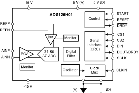
The ADS125H01 is a ±20-V input, 24-bit, delta-sigma (ΔΣ) analog-to-digital converter (ADC). The ADC features a low-noise programmable gain amplifier (PGA), a clock oscillator, and signal or reference out-of-range monitors.

The integration of a wide input range, ±18-V supply PGA and an ADC into a single package reduces board area up to 50% compared to discrete solutions.

Programmable attenuation and gain of 0.125 to 128 (corresponding to an equivalent input range from ±20 V to ±20 mV) eliminates the need for an external attenuator or external gain stages. A 1-GΩ minimum input impedance reduces error resulting from sensor loading. Additionally, the low-noise and low-drift performance allow direct connections to strain-gauge bridge and thermocouple sensors that are affected by high common-mode voltage.

The digital filter is programmable over a wide range from 2.5 SPS to 40 kSPS. Attenuation of 50-Hz and 60-Hz line cycle noise for data rates ≤ 50 SPS or 60 SPS reduces measurement error. In most data rates, the filter provides no-latency conversion data for high data throughput during external channel sequencing.

The ADS125H01 is housed in a 5-mm × 5-mm VQFN package and is fully specified over the –40°C to +125°C temperature range.

Device Information(1)
PART NUMBER PACKAGEBODY SIZE (NOM)
ADS125H01VQFN (32)5.00 mm × 5.00 mm
For all available packages, see the orderable addendum at the end of the data sheet.
GUID-96F4EB1D-1516-49DC-9C82-AB361C74C011-low.gif Functional Block Diagram