SLUSCM3K June 2016 – July 2020 BQ77904 , BQ77905
PRODUCTION DATA
- 1 Features
- 2 Applications
- 3 Description
- 4 Revision History
- 5 Device Comparison
- 6 Pin Configuration and Functions
- 7 Specifications
-
8 Detailed Description
- 8.1 Overview
- 8.2 Functional Block Diagram
- 8.3
Feature Description
- 8.3.1 Protection Summary
- 8.3.2
Fault Operation
- 8.3.2.1 Operation in OV
- 8.3.2.2 Operation in UV
- 8.3.2.3 Operation in OW
- 8.3.2.4 Operation in OCD1
- 8.3.2.5 Operation in OCD2
- 8.3.2.6 Operation in SCD
- 8.3.2.7 Overcurrent Recovery Timer
- 8.3.2.8 Load Removal Detection
- 8.3.2.9 Load Removal Detection in UV
- 8.3.2.10 Operation in OTC
- 8.3.2.11 Operation in OTD
- 8.3.2.12 Operation in UTC
- 8.3.2.13 Operation in UTD
- 8.3.3 Protection Response and Recovery Summary
- 8.3.4 Configuration CRC Check and Comparator Built-In-Self-Test
- 8.3.5 Fault Detection Method
- 8.3.6 State Comparator
- 8.3.7 DSG FET Driver Operation
- 8.3.8 CHG FET Driver Operation
- 8.3.9 External Override of CHG and DSG Drivers
- 8.3.10 Configuring 3-S, 4-S, or 5-S Mode
- 8.3.11 Stacking Implementations
- 8.3.12 Zero-Volt Battery Charging Inhibition
- 8.4 Device Functional Modes
- 9 Application and Implementation
- 10Power Supply Recommendations
- 11Layout
- 12Device and Documentation Support
- 13Mechanical, Packaging, and Orderable Information
Package Options
Mechanical Data (Package|Pins)
- PW|20
Thermal pad, mechanical data (Package|Pins)
Orderable Information
8.3.11 Stacking Implementations
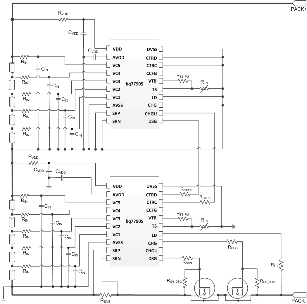
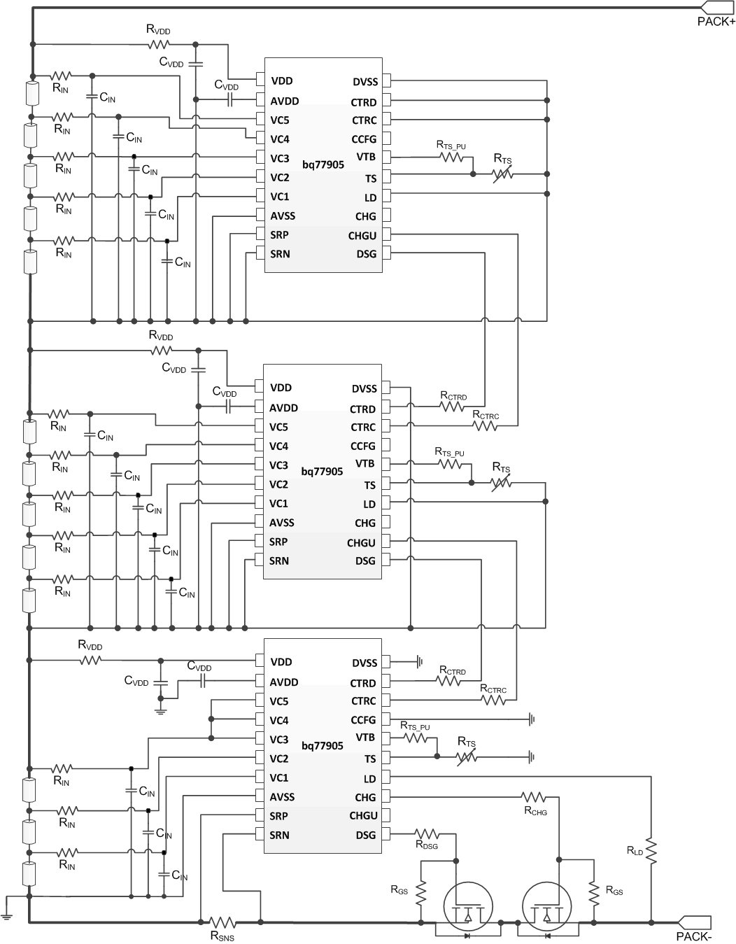
Higher than 5-S cell packs may be supported by daisy-chaining multiple devices. Each device ensures OV, UV, OTC, OTD, UTC, and UTD protections of its directly monitored cells, while any fault conditions automatically disable the global CHG and/or DSG FET driver. Note that upper devices do not provide OCD1, OCD2, or SCD protections, as these are based on pack current. For the BQ77904 and BQ77905 devices used on the upper stack, the SRP and SRN pins should be shorted to prevent false detection.
Table 8-6 Stacking Implementation Configurations
| CONFIGURATION | CHG PIN | CHGU PIN |
|---|---|---|
| Bottom or single device | Connect to CHG FET | Leave unconnected |
| Upper stack | Leave unconnected | Connect to CTRC of the lower device |
To configure higher-cell packs, follow this procedure:
- Each device must have a connection on at least three lowest-cell input pins.
- TI recommends to connect a higher-cell count to the upper devices (for example, for a 7-S configuration, connect four cells on the upper device and three cells on the bottom device). This provides a stronger CRTx signal to the bottom device.
- Ensure that each device’s CCFG pin is configured appropriately for its specific number of cells (three, four, or five cells).
- For the bottom device, the CHG pin should be used to drive the CHG FET and leave the CHGU pin unconnected. For the upper device, the CHGU pin should be used to connect to lower device’s CTRC pin with a RCTRx and leave the CHG pin unconnected.
- Connect the upper DSG pins with a RCTRx to the immediate lower device CTRD pin.
- All upper devices should have the SRP and SRN to its AVSS pin.
- If load removal is not used for UV recovery, connect the upper device LD pin to its AVSS pin, as shown in Figure 8-9 and Figure 8-10. Otherwise, refer to Figure 9-7 for proper LD connection.
 Figure 8-9 10S Pack Using Two BQ77905 Devices
 Figure 8-10 13S Pack Using Three BQ77905 Devices