SLASEO0C July   2018  – August 2025 DAC61416 , DAC71416 , DAC81416

PRODUCTION DATA  

  1.   1
  2. Features
  3. Applications
  4. Description
  5. Pin Configuration and Functions
  6. Specifications
    1. 5.1 Absolute Maximum Ratings
    2. 5.2 ESD Ratings
    3. 5.3 Recommended Operating Conditions
    4. 5.4 Thermal Information
    5. 5.5 Electrical Characteristics
    6. 5.6 Timing Requirements
    7. 5.7 Timing Diagrams
    8. 5.8 Typical Characteristics
  7. Detailed Description
    1. 6.1 Overview
    2. 6.2 Functional Block Diagram
    3. 6.3 Feature Description
      1. 6.3.1 Digital-to-Analog Converter (DAC) Architecture
        1. 6.3.1.1 DAC Transfer Function
        2. 6.3.1.2 DAC Register Structure
          1. 6.3.1.2.1 DAC Register Synchronous and Asynchronous Updates
          2. 6.3.1.2.2 Broadcast DAC Register
          3. 6.3.1.2.3 Clear DAC Operation
      2. 6.3.2 Internal Reference
      3. 6.3.3 Device Reset Options
        1. 6.3.3.1 Power-On Reset (POR)
        2. 6.3.3.2 Hardware Reset
        3. 6.3.3.3 Software Reset
      4. 6.3.4 Thermal Protection
        1. 6.3.4.1 Analog Temperature Sensor: TEMPOUT Pin
        2. 6.3.4.2 Thermal Shutdown
    4. 6.4 Device Functional Modes
      1. 6.4.1 Toggle Mode
      2. 6.4.2 Differential Mode
      3. 6.4.3 Power-Down Mode
    5. 6.5 Programming
      1. 6.5.1 Stand-Alone Operation
        1. 6.5.1.1 Streaming Mode Operation
      2. 6.5.2 Daisy-Chain Operation
      3. 6.5.3 Frame Error Checking
  8. Register Maps
  9. Application and Implementation
    1. 8.1 Application Information
    2. 8.2 Typical Application
      1. 8.2.1 Design Requirements
      2. 8.2.2 Detailed Design Procedure
      3. 8.2.3 Application Curves
    3. 8.3 Power Supply Recommendations
    4. 8.4 Layout
      1. 8.4.1 Layout Guidelines
      2. 8.4.2 Layout Example
  10. Device and Documentation Support
    1. 9.1 Device Support
      1. 9.1.1 Development Support
    2. 9.2 Documentation Support
      1. 9.2.1 Related Documentation
    3. 9.3 Receiving Notification of Documentation Updates
    4. 9.4 Support Resources
    5. 9.5 Trademarks
    6. 9.6 Electrostatic Discharge Caution
    7. 9.7 Glossary
  11. 10Revision History
  12. 11Mechanical, Packaging, and Orderable Information

Package Options

Refer to the PDF data sheet for device specific package drawings

Mechanical Data (Package|Pins)
  • RHA|40
Thermal pad, mechanical data (Package|Pins)
Orderable Information

Differential Mode

Each DAC pair in the device are independently configurable to operate as a differential output pair. The differential output of a DACx-y pair is updated by writing to the DACx channel. For proper operation, configure the two DAC pairs to the same output range before enabling differential mode. Figure 6-2 and Figure 6-3 show the ideal differential output voltages (VDIFF) and common mode voltages (VCM) for a DAC differential pair configured for ±20-V and 0 to 40-V operation, respectively.

After being configured as a differential output, set the DACx-y pair for toggle operation by updating the DACx toggle registers; see Section 6.4.1.

Imbalances between the two differential signals result in common-mode and amplitude errors. The device incorporates an offset register that enables the user to introduce a voltage offset to the DACy channel of the DACx-y differential pair to compensate for a dc offset error between the two channels. The offset compensation gives approximately a ±0.2%FSR adjustment window. Rewrite the differential DAC data register after an update to the offset register.
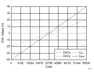
DAC61416 DAC71416 DAC81416 Differential Bipolar
                        Output (16-Bit): ±20-V Output RangeFigure 6-2 Differential Bipolar Output (16-Bit):
±20-V Output Range
DAC61416 DAC71416 DAC81416 Differential Unipolar
                        Output (16-Bit): 0-V to 40-V Output
                        RangeFigure 6-3 Differential Unipolar Output (16-Bit):
0-V to 40-V Output Range