SLVSE65C July   2018  – December 2023 DRV8847

PRODUCTION DATA  

  1.   1
  2. Features
  3. Applications
  4. Description
  5. Revision History
  6. Pin Configuration and Functions
  7. Specifications
    1. 6.1 Absolute Maximum Ratings
    2. 6.2 ESD Ratings
    3. 6.3 Recommended Operating Conditions
    4. 6.4 Thermal Information
    5. 6.5 Electrical Characteristics
    6. 6.6 I2C Timing Requirements
    7. 6.7 Typical Characteristics
  8. Detailed Description
    1. 7.1 Overview
    2. 7.2 Functional Block Diagram
    3. 7.3 Feature Description
      1. 7.3.1 PWM Motor Drivers
      2. 7.3.2 Bridge Operation
        1. 7.3.2.1 Forward Operation
        2. 7.3.2.2 Reverse Operation
        3. 7.3.2.3 Coast Operation (Fast Decay)
        4. 7.3.2.4 Brake Operation (Slow Decay)
      3. 7.3.3 Bridge Control
        1. 7.3.3.1 4-Pin Interface
        2. 7.3.3.2 2-Pin Interface
        3. 7.3.3.3 Parallel Bridge Interface
        4. 7.3.3.4 Independent Bridge Interface
      4. 7.3.4 Current Regulation
      5. 7.3.5 Current Recirculation and Decay Modes
      6. 7.3.6 Torque Scalar
      7. 7.3.7 Stepping Modes
        1. 7.3.7.1 Full-Stepping Mode (4-Pin Interface)
        2. 7.3.7.2 Full-Stepping Mode (2-Pin Interface)
        3. 7.3.7.3 Half-Stepping Mode (With Non-Driving Fast Decay)
        4. 7.3.7.4 Half-Stepping Mode (With Non-Driving Slow Decay)
      8. 7.3.8 Motor Driver Protection Circuits
        1. 7.3.8.1 Overcurrent Protection (OCP)
          1. 7.3.8.1.1 OCP Automatic Retry (Hardware Device and Software Device (OCPR = 0b))
          2. 7.3.8.1.2 OCP Latch Mode (Software Device (OCPR = 1b))
          3. 7.3.8.1.3 42
        2. 7.3.8.2 Thermal Shutdown (TSD)
        3. 7.3.8.3 VM Undervoltage Lockout (VM_UVLO)
        4. 7.3.8.4 Open Load Detection (OLD)
          1. 7.3.8.4.1 Full-Bridge Open Load Detection
          2. 7.3.8.4.2 Load Connected to VM
          3. 7.3.8.4.3 Load Connected to GND
    4. 7.4 Device Functional Modes
    5. 7.5 Programming
      1. 7.5.1 I2C Communication
        1. 7.5.1.1 I2C Write
        2. 7.5.1.2 I2C Read
      2. 7.5.2 Multi-Slave Operation
    6. 7.6 Register Map
      1. 7.6.1 Slave Address Register (Address = 0x00) [reset = 0x60]
      2. 7.6.2 IC1 Control Register (Address = 0x01) [reset = 0x00]
      3. 7.6.3 IC2 Control Register (Address = 0x02) [reset = 0x00]
      4. 7.6.4 Slew-Rate and Fault Status-1 Register (Address = 0x03) [reset = 0x40]
      5. 7.6.5 Fault Status-2 Register (Address = 0x04) [reset = 0x00]
  9. Application and Implementation
    1. 8.1 Application Information
    2. 8.2 Typical Application
      1. 8.2.1 Stepper Motor Application
        1. 8.2.1.1 Design Requirements
        2. 8.2.1.2 Detailed Design Procedure
          1. 8.2.1.2.1 Stepping Modes
            1. 8.2.1.2.1.1 Full-Stepping Operation
            2. 8.2.1.2.1.2 Half-Stepping Operation with Fast Decay
            3. 8.2.1.2.1.3 Half-Stepping Operation with Slow Decay
          2. 8.2.1.2.2 Current Regulation
        3. 8.2.1.3 Application Curves
      2. 8.2.2 Dual BDC Motor Application
        1. 8.2.2.1 Design Requirements
        2. 8.2.2.2 Detailed Design Procedure
          1. 8.2.2.2.1 Motor Voltage
          2. 8.2.2.2.2 Current Regulation
          3. 8.2.2.2.3 Sense Resistor
      3. 8.2.3 Open Load Implementation
        1. 8.2.3.1 Open Load Detection Circuit
        2. 8.2.3.2 OLD for Ground Connected Load
          1. 8.2.3.2.1 Half Bridge Open
          2. 8.2.3.2.2 Half Bridge Short
          3. 8.2.3.2.3 Load Connected
        3. 8.2.3.3 OLD for Supply (VM) Connected Load
          1. 8.2.3.3.1 Half Bridge Open
          2. 8.2.3.3.2 Half Bridge Short
          3. 8.2.3.3.3 Load Connected
        4. 8.2.3.4 OLD for Full Bridge Connected Load
          1. 8.2.3.4.1 Full Bridge Open
            1. 8.2.3.4.1.1 High side comparator of half-bridge-1 (OL1_HS)
            2. 8.2.3.4.1.2 Low side comparator of half-bridge-2 (OL2_LS)
          2. 8.2.3.4.2 Full Bridge Short
            1. 8.2.3.4.2.1 High side comparator of half-bridge-1 (OL1_HS)
            2. 8.2.3.4.2.2 Low side comparator of half-bridge-2 (OL2_LS)
          3. 8.2.3.4.3 Load Connected in Full Bridge
            1. 8.2.3.4.3.1 High side comparator of half-bridge-1 (OL1_HS)
            2. 8.2.3.4.3.2 Low side comparator of half-bridge-2 (OL2_LS)
  10.   Power Supply Recommendations
    1. 9.1 Bulk Capacitance Sizing
  11. Layout
    1. 9.1 Layout Guidelines
    2. 9.2 Layout Example
    3. 9.3 Thermal Considerations
      1. 9.3.1 Maximum Output Current
      2. 9.3.2 Thermal Protection
    4. 9.4 Power Dissipation
  12. 10Device and Documentation Support
    1. 10.1 Device Support (Optional)
      1. 10.1.1 Development Support (Optional)
      2. 10.1.2 Device Nomenclature (Optional)
    2. 10.2 Documentation Support
      1. 10.2.1 Related Documentation
    3. 10.3 Receiving Notification of Documentation Updates
    4. 10.4 Community Resources
    5. 10.5 Trademarks
  13. 11Mechanical, Packaging, and Orderable Information

Package Options

Refer to the PDF data sheet for device specific package drawings

Mechanical Data (Package|Pins)
  • PW|16
  • PWP|16
  • RTE|16
Thermal pad, mechanical data (Package|Pins)
Orderable Information

Multi-Slave Operation

Multi-slave operation is used to control multiple DRV8847S devices through one I2C line as shown in Figure 7-25. The default device address of the DRV8847 device is 0x60 (7-bit address). Therefore, any DRV8847S device can be accessed using this address. The steps for multi-slave configuration for programming device-1 out of 4 connected devices (as shown in Figure 7-25) are as follows:
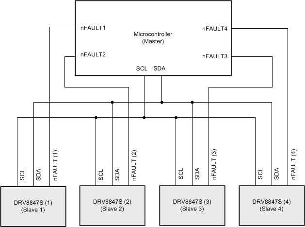
GUID-4178C301-D1E1-48E8-995B-3F6640B8DFB7-low.gifFigure 7-25 Multi-Slave Operation of DRV8847S
  • The DRV8847S device variant is configured for multi-slave operation by writing the DISFLT bit (IC2_CON register) of all connected devices to 1b. This step will disable the nFAULT output pin of all DRV8847S, to avoid any race condition between master and slave I2C device.
  • Pull the nFAULT pins (nFAULT2, nFAULT3, and nFAULT4 pins) of three devices (2, 3, and 4) to low to release the I2C buses of the slave device (device-2, device-3 and device-4). Now only device-1 is connected to master.
  • Since, only one device, DRV8847S (1), is connected to the controller, and, therefore, its slave address can be reprogrammed from default 0x60 (7-bit address) to another unique address.
  • Similarly, the slave address (SLAVE_ADDR) of the other three devices (device-2, device-3 and device-4) can be reprogrammed sequentially to unique addresses by a combination of nFAULT pins.
  • When all slave addresses are reprogrammed, write the DISFLT bit to 0b (IC2_CON register). This will enable the nFAULT output pin for fault flagging.
  • All the nFAULT pins are released and a multi-slave setup is complete. Now all connected slave devices can be accessed using the newly reprogrammed address.
  • The above steps should be repeated for any device in case of a power reset (nSLEEP). .