SLVSE65C July   2018  – December 2023 DRV8847

PRODUCTION DATA  

  1.   1
  2. Features
  3. Applications
  4. Description
  5. Revision History
  6. Pin Configuration and Functions
  7. Specifications
    1. 6.1 Absolute Maximum Ratings
    2. 6.2 ESD Ratings
    3. 6.3 Recommended Operating Conditions
    4. 6.4 Thermal Information
    5. 6.5 Electrical Characteristics
    6. 6.6 I2C Timing Requirements
    7. 6.7 Typical Characteristics
  8. Detailed Description
    1. 7.1 Overview
    2. 7.2 Functional Block Diagram
    3. 7.3 Feature Description
      1. 7.3.1 PWM Motor Drivers
      2. 7.3.2 Bridge Operation
        1. 7.3.2.1 Forward Operation
        2. 7.3.2.2 Reverse Operation
        3. 7.3.2.3 Coast Operation (Fast Decay)
        4. 7.3.2.4 Brake Operation (Slow Decay)
      3. 7.3.3 Bridge Control
        1. 7.3.3.1 4-Pin Interface
        2. 7.3.3.2 2-Pin Interface
        3. 7.3.3.3 Parallel Bridge Interface
        4. 7.3.3.4 Independent Bridge Interface
      4. 7.3.4 Current Regulation
      5. 7.3.5 Current Recirculation and Decay Modes
      6. 7.3.6 Torque Scalar
      7. 7.3.7 Stepping Modes
        1. 7.3.7.1 Full-Stepping Mode (4-Pin Interface)
        2. 7.3.7.2 Full-Stepping Mode (2-Pin Interface)
        3. 7.3.7.3 Half-Stepping Mode (With Non-Driving Fast Decay)
        4. 7.3.7.4 Half-Stepping Mode (With Non-Driving Slow Decay)
      8. 7.3.8 Motor Driver Protection Circuits
        1. 7.3.8.1 Overcurrent Protection (OCP)
          1. 7.3.8.1.1 OCP Automatic Retry (Hardware Device and Software Device (OCPR = 0b))
          2. 7.3.8.1.2 OCP Latch Mode (Software Device (OCPR = 1b))
          3. 7.3.8.1.3 42
        2. 7.3.8.2 Thermal Shutdown (TSD)
        3. 7.3.8.3 VM Undervoltage Lockout (VM_UVLO)
        4. 7.3.8.4 Open Load Detection (OLD)
          1. 7.3.8.4.1 Full-Bridge Open Load Detection
          2. 7.3.8.4.2 Load Connected to VM
          3. 7.3.8.4.3 Load Connected to GND
    4. 7.4 Device Functional Modes
    5. 7.5 Programming
      1. 7.5.1 I2C Communication
        1. 7.5.1.1 I2C Write
        2. 7.5.1.2 I2C Read
      2. 7.5.2 Multi-Slave Operation
    6. 7.6 Register Map
      1. 7.6.1 Slave Address Register (Address = 0x00) [reset = 0x60]
      2. 7.6.2 IC1 Control Register (Address = 0x01) [reset = 0x00]
      3. 7.6.3 IC2 Control Register (Address = 0x02) [reset = 0x00]
      4. 7.6.4 Slew-Rate and Fault Status-1 Register (Address = 0x03) [reset = 0x40]
      5. 7.6.5 Fault Status-2 Register (Address = 0x04) [reset = 0x00]
  9. Application and Implementation
    1. 8.1 Application Information
    2. 8.2 Typical Application
      1. 8.2.1 Stepper Motor Application
        1. 8.2.1.1 Design Requirements
        2. 8.2.1.2 Detailed Design Procedure
          1. 8.2.1.2.1 Stepping Modes
            1. 8.2.1.2.1.1 Full-Stepping Operation
            2. 8.2.1.2.1.2 Half-Stepping Operation with Fast Decay
            3. 8.2.1.2.1.3 Half-Stepping Operation with Slow Decay
          2. 8.2.1.2.2 Current Regulation
        3. 8.2.1.3 Application Curves
      2. 8.2.2 Dual BDC Motor Application
        1. 8.2.2.1 Design Requirements
        2. 8.2.2.2 Detailed Design Procedure
          1. 8.2.2.2.1 Motor Voltage
          2. 8.2.2.2.2 Current Regulation
          3. 8.2.2.2.3 Sense Resistor
      3. 8.2.3 Open Load Implementation
        1. 8.2.3.1 Open Load Detection Circuit
        2. 8.2.3.2 OLD for Ground Connected Load
          1. 8.2.3.2.1 Half Bridge Open
          2. 8.2.3.2.2 Half Bridge Short
          3. 8.2.3.2.3 Load Connected
        3. 8.2.3.3 OLD for Supply (VM) Connected Load
          1. 8.2.3.3.1 Half Bridge Open
          2. 8.2.3.3.2 Half Bridge Short
          3. 8.2.3.3.3 Load Connected
        4. 8.2.3.4 OLD for Full Bridge Connected Load
          1. 8.2.3.4.1 Full Bridge Open
            1. 8.2.3.4.1.1 High side comparator of half-bridge-1 (OL1_HS)
            2. 8.2.3.4.1.2 Low side comparator of half-bridge-2 (OL2_LS)
          2. 8.2.3.4.2 Full Bridge Short
            1. 8.2.3.4.2.1 High side comparator of half-bridge-1 (OL1_HS)
            2. 8.2.3.4.2.2 Low side comparator of half-bridge-2 (OL2_LS)
          3. 8.2.3.4.3 Load Connected in Full Bridge
            1. 8.2.3.4.3.1 High side comparator of half-bridge-1 (OL1_HS)
            2. 8.2.3.4.3.2 Low side comparator of half-bridge-2 (OL2_LS)
  10.   Power Supply Recommendations
    1. 9.1 Bulk Capacitance Sizing
  11. Layout
    1. 9.1 Layout Guidelines
    2. 9.2 Layout Example
    3. 9.3 Thermal Considerations
      1. 9.3.1 Maximum Output Current
      2. 9.3.2 Thermal Protection
    4. 9.4 Power Dissipation
  12. 10Device and Documentation Support
    1. 10.1 Device Support (Optional)
      1. 10.1.1 Development Support (Optional)
      2. 10.1.2 Device Nomenclature (Optional)
    2. 10.2 Documentation Support
      1. 10.2.1 Related Documentation
    3. 10.3 Receiving Notification of Documentation Updates
    4. 10.4 Community Resources
    5. 10.5 Trademarks
  13. 11Mechanical, Packaging, and Orderable Information

Package Options

Refer to the PDF data sheet for device specific package drawings

Mechanical Data (Package|Pins)
  • PW|16
  • PWP|16
  • RTE|16
Thermal pad, mechanical data (Package|Pins)
Orderable Information

Current Recirculation and Decay Modes

During PWM current trip operation, the H-bridge is enabled to drive current through the motor winding until the trip threshold of the current regulation is reached. After the trip current threshold is reached, the drive current is interrupted, but, because of the inductive nature of the motor, the current must continue to flow for some time. This continuous flow of current is called recirculation current. A mixed decay allows better current regulation by optimizing the current ripple by using fast and slow decay.

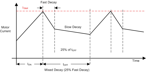
Mixed decay is a combination of fast and slow decay modes. In fast decay mode, the anti-parallel diodes of the opposite FETs are conducting on to let the current decay faster as shown in Figure 7-12 (see case 2). In slow decay mode, the winding current is recirculated by enabling both low-side FETs in the bridge (see case 3 in Figure 7-12). Mixed decay starts with fast decay, and then goes to slow decay. In the DRV8847 device, the mixed decay ratio is 25% fast decay and 75% slow decay as shown in Figure 7-13.

GUID-9F70C4B9-E4D1-48FE-AAFF-ECC8C4F421BF-low.gifFigure 7-12 Decay Modes
GUID-A3845DAA-FD7D-4218-96F8-45B55DDE9549-low.gifFigure 7-13 Mixed Decay
Note:

The current regulation scheme uses a single sense resistor and hence always works for two-half bridges even when used in an "Independent Bridge Interface". It is recommended that current regulations not be used for loads using independent half bridges.