SLVSE65C July   2018  – December 2023 DRV8847

PRODUCTION DATA  

  1.   1
  2. Features
  3. Applications
  4. Description
  5. Revision History
  6. Pin Configuration and Functions
  7. Specifications
    1. 6.1 Absolute Maximum Ratings
    2. 6.2 ESD Ratings
    3. 6.3 Recommended Operating Conditions
    4. 6.4 Thermal Information
    5. 6.5 Electrical Characteristics
    6. 6.6 I2C Timing Requirements
    7. 6.7 Typical Characteristics
  8. Detailed Description
    1. 7.1 Overview
    2. 7.2 Functional Block Diagram
    3. 7.3 Feature Description
      1. 7.3.1 PWM Motor Drivers
      2. 7.3.2 Bridge Operation
        1. 7.3.2.1 Forward Operation
        2. 7.3.2.2 Reverse Operation
        3. 7.3.2.3 Coast Operation (Fast Decay)
        4. 7.3.2.4 Brake Operation (Slow Decay)
      3. 7.3.3 Bridge Control
        1. 7.3.3.1 4-Pin Interface
        2. 7.3.3.2 2-Pin Interface
        3. 7.3.3.3 Parallel Bridge Interface
        4. 7.3.3.4 Independent Bridge Interface
      4. 7.3.4 Current Regulation
      5. 7.3.5 Current Recirculation and Decay Modes
      6. 7.3.6 Torque Scalar
      7. 7.3.7 Stepping Modes
        1. 7.3.7.1 Full-Stepping Mode (4-Pin Interface)
        2. 7.3.7.2 Full-Stepping Mode (2-Pin Interface)
        3. 7.3.7.3 Half-Stepping Mode (With Non-Driving Fast Decay)
        4. 7.3.7.4 Half-Stepping Mode (With Non-Driving Slow Decay)
      8. 7.3.8 Motor Driver Protection Circuits
        1. 7.3.8.1 Overcurrent Protection (OCP)
          1. 7.3.8.1.1 OCP Automatic Retry (Hardware Device and Software Device (OCPR = 0b))
          2. 7.3.8.1.2 OCP Latch Mode (Software Device (OCPR = 1b))
          3. 7.3.8.1.3 42
        2. 7.3.8.2 Thermal Shutdown (TSD)
        3. 7.3.8.3 VM Undervoltage Lockout (VM_UVLO)
        4. 7.3.8.4 Open Load Detection (OLD)
          1. 7.3.8.4.1 Full-Bridge Open Load Detection
          2. 7.3.8.4.2 Load Connected to VM
          3. 7.3.8.4.3 Load Connected to GND
    4. 7.4 Device Functional Modes
    5. 7.5 Programming
      1. 7.5.1 I2C Communication
        1. 7.5.1.1 I2C Write
        2. 7.5.1.2 I2C Read
      2. 7.5.2 Multi-Slave Operation
    6. 7.6 Register Map
      1. 7.6.1 Slave Address Register (Address = 0x00) [reset = 0x60]
      2. 7.6.2 IC1 Control Register (Address = 0x01) [reset = 0x00]
      3. 7.6.3 IC2 Control Register (Address = 0x02) [reset = 0x00]
      4. 7.6.4 Slew-Rate and Fault Status-1 Register (Address = 0x03) [reset = 0x40]
      5. 7.6.5 Fault Status-2 Register (Address = 0x04) [reset = 0x00]
  9. Application and Implementation
    1. 8.1 Application Information
    2. 8.2 Typical Application
      1. 8.2.1 Stepper Motor Application
        1. 8.2.1.1 Design Requirements
        2. 8.2.1.2 Detailed Design Procedure
          1. 8.2.1.2.1 Stepping Modes
            1. 8.2.1.2.1.1 Full-Stepping Operation
            2. 8.2.1.2.1.2 Half-Stepping Operation with Fast Decay
            3. 8.2.1.2.1.3 Half-Stepping Operation with Slow Decay
          2. 8.2.1.2.2 Current Regulation
        3. 8.2.1.3 Application Curves
      2. 8.2.2 Dual BDC Motor Application
        1. 8.2.2.1 Design Requirements
        2. 8.2.2.2 Detailed Design Procedure
          1. 8.2.2.2.1 Motor Voltage
          2. 8.2.2.2.2 Current Regulation
          3. 8.2.2.2.3 Sense Resistor
      3. 8.2.3 Open Load Implementation
        1. 8.2.3.1 Open Load Detection Circuit
        2. 8.2.3.2 OLD for Ground Connected Load
          1. 8.2.3.2.1 Half Bridge Open
          2. 8.2.3.2.2 Half Bridge Short
          3. 8.2.3.2.3 Load Connected
        3. 8.2.3.3 OLD for Supply (VM) Connected Load
          1. 8.2.3.3.1 Half Bridge Open
          2. 8.2.3.3.2 Half Bridge Short
          3. 8.2.3.3.3 Load Connected
        4. 8.2.3.4 OLD for Full Bridge Connected Load
          1. 8.2.3.4.1 Full Bridge Open
            1. 8.2.3.4.1.1 High side comparator of half-bridge-1 (OL1_HS)
            2. 8.2.3.4.1.2 Low side comparator of half-bridge-2 (OL2_LS)
          2. 8.2.3.4.2 Full Bridge Short
            1. 8.2.3.4.2.1 High side comparator of half-bridge-1 (OL1_HS)
            2. 8.2.3.4.2.2 Low side comparator of half-bridge-2 (OL2_LS)
          3. 8.2.3.4.3 Load Connected in Full Bridge
            1. 8.2.3.4.3.1 High side comparator of half-bridge-1 (OL1_HS)
            2. 8.2.3.4.3.2 Low side comparator of half-bridge-2 (OL2_LS)
  10.   Power Supply Recommendations
    1. 9.1 Bulk Capacitance Sizing
  11. Layout
    1. 9.1 Layout Guidelines
    2. 9.2 Layout Example
    3. 9.3 Thermal Considerations
      1. 9.3.1 Maximum Output Current
      2. 9.3.2 Thermal Protection
    4. 9.4 Power Dissipation
  12. 10Device and Documentation Support
    1. 10.1 Device Support (Optional)
      1. 10.1.1 Development Support (Optional)
      2. 10.1.2 Device Nomenclature (Optional)
    2. 10.2 Documentation Support
      1. 10.2.1 Related Documentation
    3. 10.3 Receiving Notification of Documentation Updates
    4. 10.4 Community Resources
    5. 10.5 Trademarks
  13. 11Mechanical, Packaging, and Orderable Information

Package Options

Refer to the PDF data sheet for device specific package drawings

Mechanical Data (Package|Pins)
  • PW|16
  • PWP|16
  • RTE|16
Thermal pad, mechanical data (Package|Pins)
Orderable Information

Parallel Bridge Interface

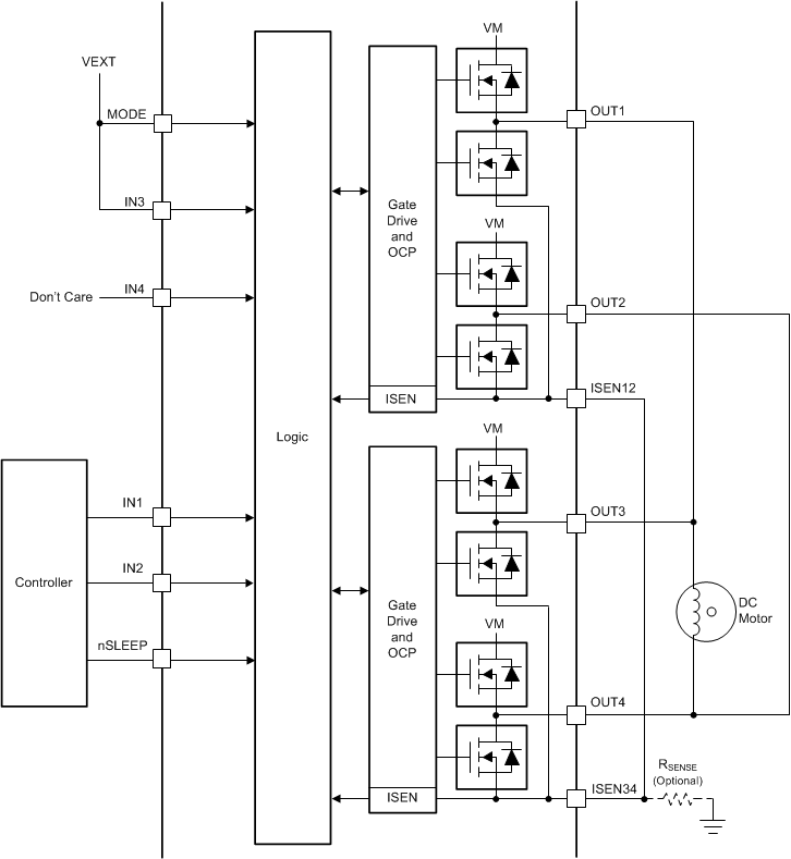
In the parallel bridge interface, the DRV8847 device is configured to drive a higher current BDC motor by using the driver in parallel to deliver twice the motor current. To go to parallel bridge interface operation, connect the MODE and IN3 pins to the external supply (3.3 V or 5 V) and use the IN1 and IN2 pins to control the driver. This mode can deliver the full functionality of the BDC motor control with all four modes (forward, reverse, coast, and brake mode).

Use this interface option for the following loads:

  • One high current BDC motor (with or without current regulation) with full functional BDC modes (forward, reverse, brake, and coast mode)
  • Two independent BDC motors operating together (with or without current regulation) with full functional BDC modes (forward, reverse, brake, and coast mode)

Table 7-5 lists the configurations for parallel bridge interface operation, and Figure 7-10 shows the application diagram for parallel bridge interface operation.

Table 7-5 Parallel Interface (MODE = 1, IN3 = 1)
nSLEEPIN1IN2IN3IN4OUT1OUT2OUT3OUT4FUNCTION (DC MOTOR)
0XXXXZZZZSleep mode
1001XZZZZMotor coast (fast decay)
1011XLHLHReverse direction
1101XHLHLForward direction
1111XLLLLMotor brake (slow decay)
GUID-4880829F-B2AF-477B-AC8D-901F583C1556-low.gifFigure 7-10 Parallel Mode Operation