SLVSE65C July   2018  – December 2023 DRV8847

PRODUCTION DATA  

  1.   1
  2. Features
  3. Applications
  4. Description
  5. Revision History
  6. Pin Configuration and Functions
  7. Specifications
    1. 6.1 Absolute Maximum Ratings
    2. 6.2 ESD Ratings
    3. 6.3 Recommended Operating Conditions
    4. 6.4 Thermal Information
    5. 6.5 Electrical Characteristics
    6. 6.6 I2C Timing Requirements
    7. 6.7 Typical Characteristics
  8. Detailed Description
    1. 7.1 Overview
    2. 7.2 Functional Block Diagram
    3. 7.3 Feature Description
      1. 7.3.1 PWM Motor Drivers
      2. 7.3.2 Bridge Operation
        1. 7.3.2.1 Forward Operation
        2. 7.3.2.2 Reverse Operation
        3. 7.3.2.3 Coast Operation (Fast Decay)
        4. 7.3.2.4 Brake Operation (Slow Decay)
      3. 7.3.3 Bridge Control
        1. 7.3.3.1 4-Pin Interface
        2. 7.3.3.2 2-Pin Interface
        3. 7.3.3.3 Parallel Bridge Interface
        4. 7.3.3.4 Independent Bridge Interface
      4. 7.3.4 Current Regulation
      5. 7.3.5 Current Recirculation and Decay Modes
      6. 7.3.6 Torque Scalar
      7. 7.3.7 Stepping Modes
        1. 7.3.7.1 Full-Stepping Mode (4-Pin Interface)
        2. 7.3.7.2 Full-Stepping Mode (2-Pin Interface)
        3. 7.3.7.3 Half-Stepping Mode (With Non-Driving Fast Decay)
        4. 7.3.7.4 Half-Stepping Mode (With Non-Driving Slow Decay)
      8. 7.3.8 Motor Driver Protection Circuits
        1. 7.3.8.1 Overcurrent Protection (OCP)
          1. 7.3.8.1.1 OCP Automatic Retry (Hardware Device and Software Device (OCPR = 0b))
          2. 7.3.8.1.2 OCP Latch Mode (Software Device (OCPR = 1b))
          3. 7.3.8.1.3 42
        2. 7.3.8.2 Thermal Shutdown (TSD)
        3. 7.3.8.3 VM Undervoltage Lockout (VM_UVLO)
        4. 7.3.8.4 Open Load Detection (OLD)
          1. 7.3.8.4.1 Full-Bridge Open Load Detection
          2. 7.3.8.4.2 Load Connected to VM
          3. 7.3.8.4.3 Load Connected to GND
    4. 7.4 Device Functional Modes
    5. 7.5 Programming
      1. 7.5.1 I2C Communication
        1. 7.5.1.1 I2C Write
        2. 7.5.1.2 I2C Read
      2. 7.5.2 Multi-Slave Operation
    6. 7.6 Register Map
      1. 7.6.1 Slave Address Register (Address = 0x00) [reset = 0x60]
      2. 7.6.2 IC1 Control Register (Address = 0x01) [reset = 0x00]
      3. 7.6.3 IC2 Control Register (Address = 0x02) [reset = 0x00]
      4. 7.6.4 Slew-Rate and Fault Status-1 Register (Address = 0x03) [reset = 0x40]
      5. 7.6.5 Fault Status-2 Register (Address = 0x04) [reset = 0x00]
  9. Application and Implementation
    1. 8.1 Application Information
    2. 8.2 Typical Application
      1. 8.2.1 Stepper Motor Application
        1. 8.2.1.1 Design Requirements
        2. 8.2.1.2 Detailed Design Procedure
          1. 8.2.1.2.1 Stepping Modes
            1. 8.2.1.2.1.1 Full-Stepping Operation
            2. 8.2.1.2.1.2 Half-Stepping Operation with Fast Decay
            3. 8.2.1.2.1.3 Half-Stepping Operation with Slow Decay
          2. 8.2.1.2.2 Current Regulation
        3. 8.2.1.3 Application Curves
      2. 8.2.2 Dual BDC Motor Application
        1. 8.2.2.1 Design Requirements
        2. 8.2.2.2 Detailed Design Procedure
          1. 8.2.2.2.1 Motor Voltage
          2. 8.2.2.2.2 Current Regulation
          3. 8.2.2.2.3 Sense Resistor
      3. 8.2.3 Open Load Implementation
        1. 8.2.3.1 Open Load Detection Circuit
        2. 8.2.3.2 OLD for Ground Connected Load
          1. 8.2.3.2.1 Half Bridge Open
          2. 8.2.3.2.2 Half Bridge Short
          3. 8.2.3.2.3 Load Connected
        3. 8.2.3.3 OLD for Supply (VM) Connected Load
          1. 8.2.3.3.1 Half Bridge Open
          2. 8.2.3.3.2 Half Bridge Short
          3. 8.2.3.3.3 Load Connected
        4. 8.2.3.4 OLD for Full Bridge Connected Load
          1. 8.2.3.4.1 Full Bridge Open
            1. 8.2.3.4.1.1 High side comparator of half-bridge-1 (OL1_HS)
            2. 8.2.3.4.1.2 Low side comparator of half-bridge-2 (OL2_LS)
          2. 8.2.3.4.2 Full Bridge Short
            1. 8.2.3.4.2.1 High side comparator of half-bridge-1 (OL1_HS)
            2. 8.2.3.4.2.2 Low side comparator of half-bridge-2 (OL2_LS)
          3. 8.2.3.4.3 Load Connected in Full Bridge
            1. 8.2.3.4.3.1 High side comparator of half-bridge-1 (OL1_HS)
            2. 8.2.3.4.3.2 Low side comparator of half-bridge-2 (OL2_LS)
  10.   Power Supply Recommendations
    1. 9.1 Bulk Capacitance Sizing
  11. Layout
    1. 9.1 Layout Guidelines
    2. 9.2 Layout Example
    3. 9.3 Thermal Considerations
      1. 9.3.1 Maximum Output Current
      2. 9.3.2 Thermal Protection
    4. 9.4 Power Dissipation
  12. 10Device and Documentation Support
    1. 10.1 Device Support (Optional)
      1. 10.1.1 Development Support (Optional)
      2. 10.1.2 Device Nomenclature (Optional)
    2. 10.2 Documentation Support
      1. 10.2.1 Related Documentation
    3. 10.3 Receiving Notification of Documentation Updates
    4. 10.4 Community Resources
    5. 10.5 Trademarks
  13. 11Mechanical, Packaging, and Orderable Information

Package Options

Refer to the PDF data sheet for device specific package drawings

Mechanical Data (Package|Pins)
  • PW|16
  • PWP|16
  • RTE|16
Thermal pad, mechanical data (Package|Pins)
Orderable Information

2-Pin Interface

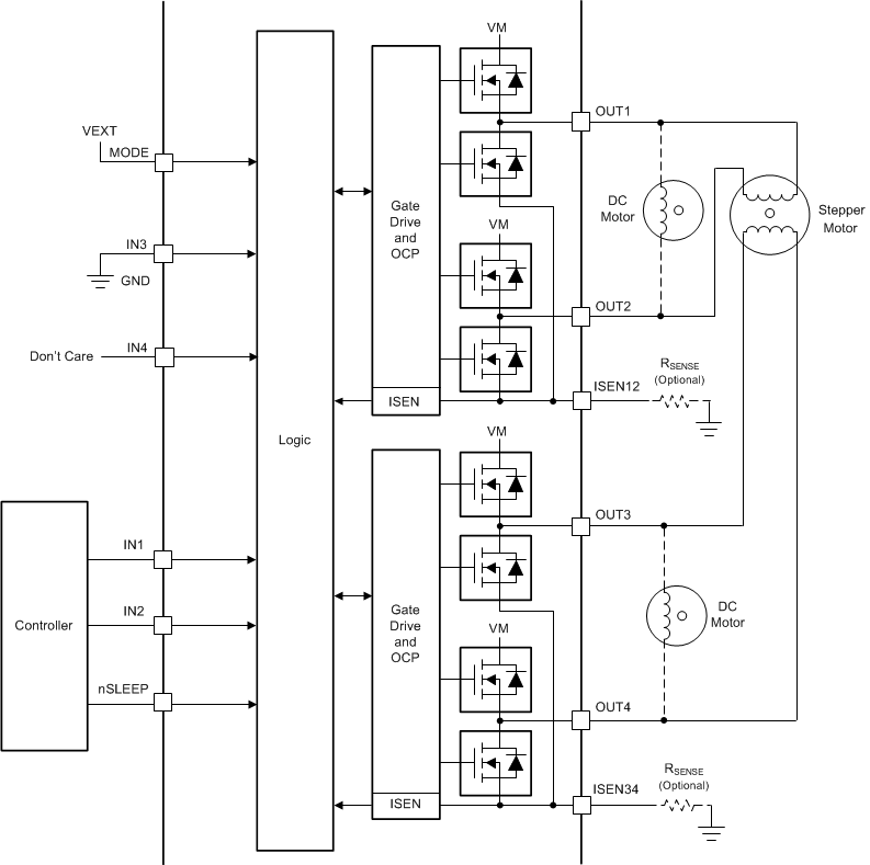
In the 2-pin interface, the DRV8847 device is configured to drive a stepper motor or two BDC motors with a lower number of control inputs from the microcontroller. To configure the 2-pin interface operation, connect the MODE pin to the external supply (3.3 V or 5 V), connect the IN3 pin to the ground, and use the IN1 and IN2 pins to control the driver. In this mode, the stepper or brushed DC motor operates in only two modes (forward mode and reverse mode) i.e. only full-step operation is supported for the stepper motor. This 2-pin interface is very useful for low GPIO applications such as refrigerator dampers. Sense resistors can be connected to the ISEN12 and ISEN34 pins for current regulation.

Use this interface option for the following loads:

  • Stepper motor in full stepping mode (with or without current regulation)
  • Single or dual BDC motor (with or without current regulation) with reduced functional BDC modes (forward and reverse mode only)

Table 7-4 lists the configurations for 2-pin interface operation and Figure 7-9 shows the application diagram for 2-pin interface operation.

Table 7-4 2-Pin Interface (MODE = 1, IN3 = 0)
nSLEEPIN1IN2IN3IN4OUT1OUT2OUT3OUT4FUNCTION (DC MOTOR)
0XXXXZZZZSleep mode
100XLHReverse direction
110XHLForward direction
100XLHReverse direction
110XHLForward direction
GUID-3C18C593-00B1-4797-B075-F26141204283-low.gifFigure 7-9 2-Pin Interface Operation
Note:

In this mode, two of the OUTx pins are always 'ON' if the device is in a non-sleep state (nSLEEP = HIGH). Therefore, to completely de-energize the motor-coils connected to OUTx pins, the user has to pull-down the nSLEEP pin.