SNOSDC0A October   2020  – December 2020 LM7310

PRODUCTION DATA  

  1. Features
  2. Applications
  3. Description
  4. Revision History
  5. Pin Configuration and Functions
  6. Specifications
    1. 6.1 Absolute Maximum Ratings
    2. 6.2 ESD Ratings
    3. 6.3 Recommended Operating Conditions
    4. 6.4 Thermal Information
    5. 6.5 Electrical Characteristics
    6. 6.6 Timing Requirements
    7. 6.7 Switching Characteristics
    8.     14
    9. 6.8 Typical Characteristics
  7. Detailed Description
    1. 7.1 Overview
    2. 7.2 Functional Block Diagram
    3. 7.3 Feature Description
      1. 7.3.1 Input Reverse Polarity Protection
      2. 7.3.2 Undervoltage Protection (UVLO & UVP)
      3. 7.3.3 Overvoltage Lockout (OVLO)
      4. 7.3.4 Inrush Current control and Fast-trip
        1. 7.3.4.1 Slew Rate (dVdt) and Inrush Current Control
        2. 7.3.4.2 Fast-Trip During Steady State
      5. 7.3.5 Analog Load Current Monitor Output
      6. 7.3.6 Reverse Current Protection
      7. 7.3.7 Overtemperature Protection (OTP)
      8. 7.3.8 Fault Response
      9. 7.3.9 Power Good Indication (PG)
    4. 7.4 Device Functional Modes
  8. Application and Implementation
    1. 8.1 Application Information
    2. 8.2 Single Device, Self-Controlled
      1. 8.2.1 Typical Application
        1. 8.2.1.1 Design Requirements
        2. 8.2.1.2 Detailed Design Procedure
          1. 8.2.1.2.1 Setting Undervoltage and Overvoltage Thresholds
          2. 8.2.1.2.2 Setting Output Voltage Rise Time (tR)
          3. 8.2.1.2.3 Setting Power Good Assertion Threshold
          4. 8.2.1.2.4 Setting Analog Current Monitor Voltage (IMON) Range
        3. 8.2.1.3 Application Curves
    3. 8.3 Active ORing
    4. 8.4 Priority Power MUXing
    5. 8.5 USB PD Port Protection
    6. 8.6 Parallel Operation
  9. Power Supply Recommendations
    1. 9.1 Transient Protection
  10. 10Layout
    1. 10.1 Layout Guidelines
    2. 10.2 Layout Example
  11. 11Device and Documentation Support
    1. 11.1 Documentation Support
      1. 11.1.1 Related Documentation
    2. 11.2 Receiving Notification of Documentation Updates
    3. 11.3 Support Resources
    4. 11.4 Trademarks
    5. 11.5 Electrostatic Discharge Caution
    6. 11.6 Glossary
  12. 12Mechanical, Packaging, and Orderable Information

Package Options

Mechanical Data (Package|Pins)
Thermal pad, mechanical data (Package|Pins)
Orderable Information
Setting Undervoltage and Overvoltage Thresholds

The supply undervoltage and overvoltage thresholds are set using the resistors R1, R2 & R3 whose values can be calculated using Equation 6 and Equation 7:

Equation 6. GUID-20200927-CA0I-TPM8-V4NF-WNDX1CBJLPSK-low.gif
Equation 7. GUID-20201002-CA0I-ZJZG-RF3Z-LKLJ3QZBZCK0-low.gif
Where VUVLO(R) is the UVLO rising threshold and VOV(R) is the OVLO rising threshold . Because R1, R2 and R3 leak the current from input supply VIN, these resistors must be selected based on the acceptable leakage current from input power supply VIN. The current drawn by R1, R2 and R3 from the power supply is IR123 = VIN / (R1 + R2 + R3). However, leakage currents due to external active components connected to the resistor string can add error to these calculations. So, the resistor string current, IR123 must be chosen to be 20 times greater than the leakage current expected on the EN/UVLO and OVLO pins.

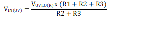
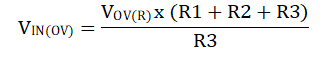
From the device electrical specifications, both the EN/UVLO and OVLO leakage currents are 0.1 μA (max), VOV(R) = 1.2 V and VUVLO(R) = 1.2 V. From design requirements, VIN(OV) = 13.2 V and VIN(UV) = 10.8 V. To solve the equation, first choose the value of R1 = 470 kΩ and use the above equations to solve for R2 = 10.7 kΩ and R3= 48 kΩ.

Using the closest standard 1% resistor values, we get R1 = 470 kΩ, R2 = 11 kΩ, and R3 = 47 kΩ.