SNAS579G March 2012 – December 2014 LMK00105
PRODUCTION DATA.
- 1 Features
- 2 Applications
- 3 Description
- 4 Revision History
- 5 Pin Configuration and Diagrams
- 6 Specifications
- 7 Detailed Description
- 8 Application and Implementation
- 9 Power Supply Recommendations
- 10Layout
- 11Device and Documentation Support
- 12Mechanical, Packaging, and Orderable Information
Package Options
Refer to the PDF data sheet for device specific package drawings
Mechanical Data (Package|Pins)
- RTW|24
Thermal pad, mechanical data (Package|Pins)
Orderable Information
8.2.1.3 Application Curves
The LMK00105 was tested using multiple low-jitter XO clock sources to evaluate the impact of the buffer’s additive phase noise/jitter. The plots on the left show the phase noise of the clock source, while the plots on the right show the total output phase noise from LMK00105 contributed by both the clock source noise and buffer additive noise. Note that the phase noise “hump” around 80 kHz offset on the phase noise plots is correlated to the XO source, which is attributed to power supply noise at this frequency.
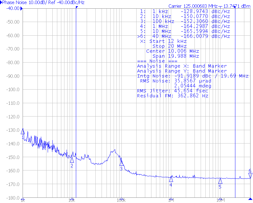 Figure 11. Phase Noise of 125-MHz Clock Source
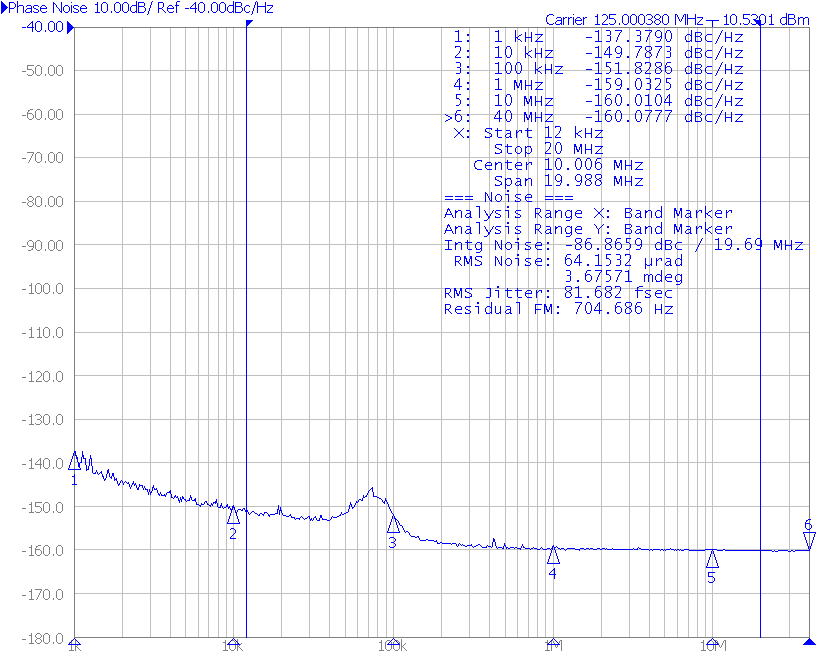 Figure 12. LMK00105 Clock Output
A low-noise 125 MHz XO clock source with 45.6 fs RMS jitter (Figure 11) was used to drive the LMK00105, resulting in in a total output phase jitter of 81.6 fs RMS (Figure 12) integrated from 12 kHz to 20 MHz. The resultant additive jitter of the buffer is 67.7 fs RMS computed using the “Square-Root of the Difference of Squares” method.
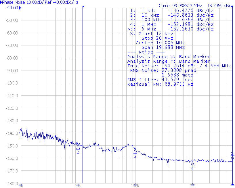 Figure 13. Phase Noise of 100-MHz Clock Source
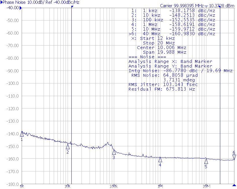 Figure 14. LMK00105 Clock Output
A low-noise 100 MHz XO clock source with 43.5 fs RMS jitter (Figure 13) was used to drive the LMK00105, resulting in a total output phase jitter of 103.1 fs RMS (Figure 14) integrated from 12 kHz to 20 MHz. The resultant additive jitter of the buffer is 93.4 fs RMS computed using the “Square-Root of the Difference of Squares” method.
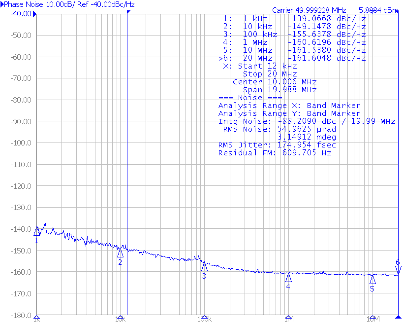 Figure 15. Phase Noise of 50-MHz Clock Source
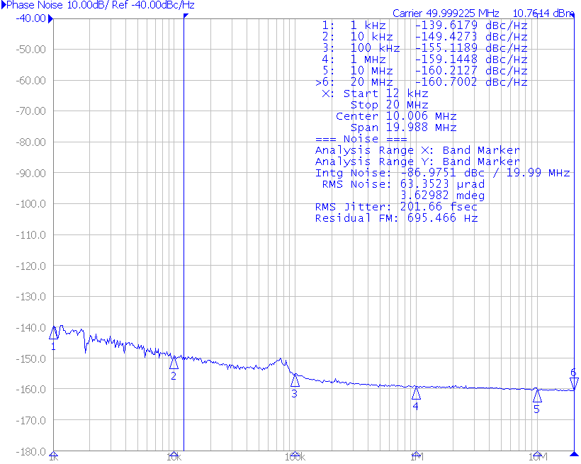 Figure 16. LMK00105 Clock Output
A divide-by-2 circuit was used with the low-noise 100-MHz XO to generate a 50-MHz clock source with 174.9fs RMS jitter (Figure 15), resulting in a total output phase jitter of 201.6 fs RMS (Figure 16) integrated from 12 kHz to 20 MHz.
In this case, the total output phase noise/jitter is highly correlated to the clock source phase noise and jitter, which prevents us from computing the true additive jitter of the buffer using the “Square-Root of the Difference of Squares” method. To accurately specify the additive jitter of the buffer at this frequency, a clock source with lower noise (compared to the DUT) would be needed for this measurement.
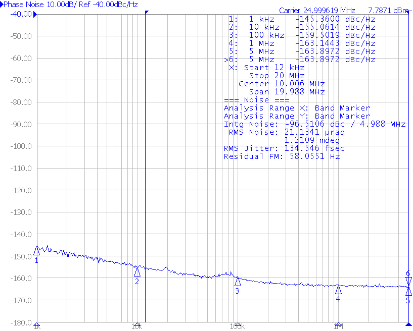 Figure 17. Phase Noise of 25-MHz Clock Source
 Figure 18. LMK00105 Clock Output
A divide-by-4 circuit was used with the low-noise 100 MHz XO to generate a 25-MHz clock source with 134.5 fs RMS (Figure 17), resulting in a total output phase jitter of 138.2 fs RMS (Figure 18) integrated from 12 kHz to 5 MHz.
In this case, the total output phase noise and jitter is highly correlated to the clock source phase noise and jitter, which prevents us from computing the true additive jitter of the buffer using the “Square-Root of the Difference of Squares” method. To accurately specify the additive jitter of the buffer at this frequency, a clock source with lower noise (compared to the DUT) would be needed for this measurement.