SNAS579G March   2012  – December 2014 LMK00105

PRODUCTION DATA.  

  1. Features
  2. Applications
  3. Description
    1.     Device Images
      1.      Functional Block Diagram
  4. Revision History
  5. Pin Configuration and Diagrams
    1.     Pin Functions
  6. Specifications
    1. 6.1 Absolute Maximum Ratings
    2. 6.2 ESD Ratings
    3. 6.3 Recommended Operating Conditions
    4. 6.4 Thermal Information
    5. 6.5 Electrical Characteristics
    6. 6.6 Typical Characteristics
  7. Detailed Description
    1. 7.1 Overview
    2. 7.2 Functional Block Diagram
    3. 7.3 Feature Description
      1. 7.3.1 Vdd and Vddo Power Supplies
      2. 7.3.2 Clock Input
        1. 7.3.2.1 Selection of Clock Input
          1. 7.3.2.1.1 CLKin/CLKin* Pins
          2. 7.3.2.1.2 OSCin/OSCout Pins
      3. 7.3.3 Clock Outputs
        1. 7.3.3.1 Output Enable Pin
        2. 7.3.3.2 Using Less than Five Outputs
    4. 7.4 Device Functional Modes
  8. Application and Implementation
    1. 8.1 Application Information
      1. 8.1.1 Clock Inputs
      2. 8.1.2 Clock Outputs
    2. 8.2 Typical Applications
      1. 8.2.1 Typical Application Block Diagram
        1. 8.2.1.1 Design Requirements
        2. 8.2.1.2 Detailed Design Procedure
        3. 8.2.1.3 Application Curves
      2. 8.2.2 Crystal Interface
        1. 8.2.2.1 Design Requirements
        2. 8.2.2.2 Detailed Design Procedure
        3. 8.2.2.3 Application Curves
  9. Power Supply Recommendations
    1. 9.1 Power Supply Filtering
    2. 9.2 Power Supply Ripple Rejection
    3. 9.3 Power Supply Bypassing
  10. 10Layout
    1. 10.1 Layout Guidelines
      1. 10.1.1 Ground Planes
      2. 10.1.2 Power Supply Pins
      3. 10.1.3 Differential Input Termination
      4. 10.1.4 Output Termination
    2. 10.2 Layout Example
    3. 10.3 Thermal Management
  11. 11Device and Documentation Support
    1. 11.1 Documentation Support
      1. 11.1.1 Differential Voltage Measurement Terminology
    2. 11.2 Trademarks
    3. 11.3 Electrostatic Discharge Caution
    4. 11.4 Glossary
  12. 12Mechanical, Packaging, and Orderable Information

Package Options

Refer to the PDF data sheet for device specific package drawings

Mechanical Data (Package|Pins)
  • RTW|24
Thermal pad, mechanical data (Package|Pins)
Orderable Information

Typical Characteristics

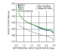
Unless otherwise specified: Vdd = Vddo = 3.3 V, TA = 20 °C, CL = 5 pF, CLKin driven differentially, input slew rate ≥ 2 V/ns.
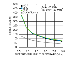
LMK00105 30180741.gifFigure 1. RMS Jitter vs. CLKin Slew Rate @ 100 MHz
LMK00105 30180742.gif
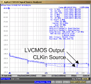
Test conditions: LVCMOS Input, slew rate ≥ 2 V/ns, CL = 5 pF in parallel with 50 Ω, BW = 1 MHz to 20 MHz
Figure 3. LVCMOS Phase Noise @ 100 MHz
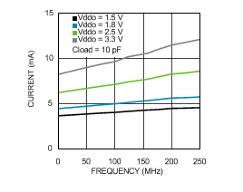
LMK00105 30180776.gifFigure 5. Iddo per Output vs Frequency
LMK00105 30180774.gifFigure 2. Noise Floor vs. CLKin Slew Rate @ 100 MHz
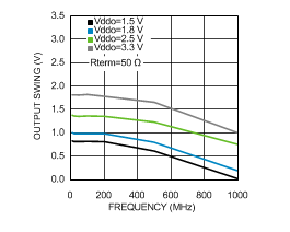
LMK00105 30180775.gifFigure 4. LVCMOS Output Swing vs. Frequency