SLLS177I March 1994 – March 2021 TL16C550C
PRODUCTION DATA
- 1 Features
- 2 Description
- 3 Revision History
- 4 Pin Configuration and Functions
-
5 Specifications
- 5.1 Absolute Maximum Ratings
- 5.2 Recommended Operating Conditions (Low Voltage - 3.3 nominal)
- 5.3 Recommended Operating Conditions (Standard Voltage - 5 V nominal)
- 5.4 Thermal Information
- 5.5 Electrical Characteristics (Low Voltage - 3.3 V nominal)
- 5.6 Electrical Characteristics (Standard Voltage - 5 V nominal)
- 5.7 System Timing Requirements
- 5.8 System Switching Characteristics
- 5.9 Baud Generator Switching Characteristics
- 5.10 Receiver Switching Characteristics
- 5.11 Transmitter Switching Characteristics
- 5.12 Modem Control Switching Characteristics
- 6 Parameter Measurement Information
-
7 Detailed Description
- 7.1 Autoflow Control (see Figure 1-1)
- 7.2 Auto-RTS (see Figure 1-1)
- 7.3 Auto-CTS (see Figure 1-1)
- 7.4 Enabling Autoflow Control and Auto-CTS
- 7.5 Auto-CTS and Auto-RTS Functional Timing
- 7.6 Functional Block Diagram
- 7.7
Principles of Operation
- 7.7.1 Accessible Registers
- 7.7.2 FIFO Control Register (FCR)
- 7.7.3 FIFO Interrupt Mode Operation
- 7.7.4 FIFO Polled Mode Operation
- 7.7.5 Interrupt Enable Register (IER)
- 7.7.6 Interrupt Identification Register (IIR)
- 7.7.7 Line Control Register (LCR)
- 7.7.8 Line Status Register (LSR)
- 7.7.9 Modem Control Register (MCR)
- 7.7.10 Modem Status Register (MSR)
- 7.7.11 Programming Baud Generator
- 7.7.12 Receiver Buffet Register (RBR)
- 7.7.13 Scratch Register
- 7.7.14 Transmitter Holding Register (THR)
- 8 Application Information
- 9 Device and Documentation Support
- 10Mechanical, Packaging, and Orderable Information
Package Options
Mechanical Data (Package|Pins)
Thermal pad, mechanical data (Package|Pins)
- PFB|48
Orderable Information
7.7.11 Programming Baud Generator
The ACE contains a programmable baud generator that takes a clock input in the range between dc and 16 MHz and divides it by a divisor in the range between 1 and (216−1).The output frequency of the baud generator is sixteen times (16 x) the baud rate. The formula for the divisor is:
Two 8-bit registers, called divisor latches, store the divisor in a 16-bit binary format. These divisor latches must be loaded during initialization of the ACE in order to ensure desired operation of the baud generator. When either of the divisor latches is loaded, a 16-bit baud counter is also loaded to prevent long counts on initial load.
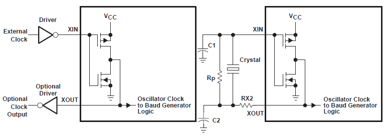
Table 7-9 and Table 7-10 illustrate the use of the baud generator with crystal frequencies of 1.8432 MHz and 3.072 MHz respectively. For baud rates of 38.4 kbits/s and below, the error obtained is very small. The accuracy of the selected baud rate is dependent on the selected crystal frequency (refer to Figure 7-5 for examples of typical clock circuits).
| DESIRED BAUD RATE | DIVISOR USED TO GENERATE 16 x CLOCK | PERCENT ERROR DIFFERENCE BETWEEN DESIRED AND ACTUAL |
|---|---|---|
| 50 | 2304 | |
| 75 | 1536 | |
| 110 | 1047 | 0.026 |
| 134.5 | 857 | 0.058 |
| 150 | 768 | |
| 300 | 384 | |
| 600 | 192 | |
| 1200 | 96 | |
| 1800 | 64 | |
| 2000 | 58 | 0.69 |
| 2400 | 48 | |
| 3600 | 32 | |
| 4800 | 24 | |
| 7200 | 16 | |
| 9600 | 12 | |
| 19200 | 6 | |
| 38400 | 3 | |
| 56000 | 2 | 2.86 |
| DESIRED BAUD RATE | DIVISOR USED TO GENERATE 16 x CLOCK | PERCENT ERROR DIFFERENCE BETWEEN DESIRED AND ACTUAL |
|---|---|---|
| 50 | 3840 | |
| 75 | 2560 | |
| 110 | 1745 | 0.026 |
| 134.5 | 1428 | 0.034 |
| 150 | 1280 | |
| 300 | 640 | |
| 600 | 320 | |
| 1200 | 160 | |
| 1800 | 107 | 0.312 |
| 2000 | 96 | |
| 2400 | 80 | |
| 3600 | 53 | 0.628 |
| 4800 | 40 | |
| 7200 | 27 | 1.23 |
| 9600 | 20 | |
| 19200 | 10 | |
| 38400 | 5 |
 Figure 7-5 Typical Clock Circuits
| CRYSTAL | RP | RX2 | C1 | C2 |
|---|---|---|---|---|
| 3.072 MHz | 1 MW | 1.5 kW | 10 − 30 pF | 40 − 60 pF |
| 1.8432 MHz | 1 MW | 1.5 kW | 10 − 30 pF | 40 − 60 pF |