SLOS191E February 1997 – July 2025 TLE2021AM , TLE2021B , TLE2021M-MIL , TLE2022AM-MIL , TLE2022BM , TLE2022M-MIL , TLE2024AM , TLE2024BM-MIL , TLE2024M
PRODUCTION DATA
- 1
- 1 Features
- 2 Description
- 3 Device Comparison Tables
- 4 Pin Configuration and Functions
-
5 Specifications
- 5.1 Absolute Maximum Ratings
- 5.2 Dissipation Ratings
- 5.3 Recommended Operating Conditions
- 5.4 Electrical Characteristics TLE2021xM, VCC = 5 V
- 5.5 Operating Characteristics TLE2021M, VCC = 5 V
- 5.6 Electrical Characteristics TLE2021xM, VCC = ±15 V
- 5.7 Operating Characteristics TLE2021M, VCC = ±15 V
- 5.8 Electrical Characteristics TLE2022xM, VCC = 5 V
- 5.9 Operating Characteristics TLE2022M, VCC = 5 V
- 5.10 Electrical Characteristics TLE2022xM, VCC = ±15 V
- 5.11 Operating Characteristics TLE2022M, VCC = ±15 V
- 5.12 Electrical Characteristics TLE2024xM, VCC = 5 V
- 5.13 Operating Characteristics TLE2024M, VCC = 5 V
- 5.14 Electrical Characteristics TLE2024xM, VCC = ±15 V
- 5.15 Operating Characteristics TLE2024M, VCC = ±15 V
- 5.16 Typical Characteristics
- 6 Parameter Measurement Information
- 7 Detailed Description
- 8 Application and Implementation
- 9 Device and Documentation Support
- 10Revision History
- 11Mechanical, Packaging, and Orderable Information
Package Options
Refer to the PDF data sheet for device specific package drawings
Mechanical Data (Package|Pins)
- FK|20
- JG|8
Thermal pad, mechanical data (Package|Pins)
Orderable Information
8.1.1 Voltage-Follower Applications
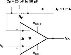
The TLE202xM circuitry includes input-protection diodes to limit the voltage across the input transistors; however, no provision is made in the circuit to limit the current if these diodes are forward biased. This condition sometimes occurs when the device is operated in the voltage-follower configuration and driven with a fast, large-signal pulse. Use a feedback resistor to limit the current to a maximum of 1mA to prevent degradation of the device. This feedback resistor forms a pole with the input capacitance of the device. For feedback resistor values greater than 10kΩ, this pole degrades the amplifier phase margin. Figure 8-1 shows that to alleviate this problem, add a capacitor (20pF to 50pF) in parallel with the feedback resistor.
 Figure 8-1 Voltage
Follower