SLOS183E February 1997 – July 2025 TLE2141 , TLE2141A , TLE2142 , TLE2142A , TLE2142AM , TLE2142AM-D , TLE2142M , TLE2142M-D , TLE2144 , TLE2144A , TLE2144AM , TLE2144M , TLE2144M-D
PRODUCTION DATA
- 1
- 1Features
- 2Applications
- 3Description
- 4Pin Configuration and Functions
-
5Specifications
- 5.1 Absolute Maximum Ratings
- 5.2 Recommended Operating Conditions
- 5.3 TLE2141C Electrical Characteristics
- 5.4 TLE2141C Operating Characteristics, VCC = 5V , TA = 25°C
- 5.5 TLE2141C Electrical Characteristics
- 5.6 TLE2141C Operating Characteristics, VCC± = ±15V , TA = 25°C
- 5.7 TLE2142C Electrical Characteristics
- 5.8 TLE2142C Operating Characteristics, VCC = 5V , TA = 25°C
- 5.9 TLE2142C Electrical Characteristics
- 5.10 TLE2142C Operating Characteristics, VCC± = ±15V , TA = 25°C
- 5.11 TLE2144C Electrical Characteristics
- 5.12 TLE2144C Operating Characteristics, VCC = 5V , TA = 25°C
- 5.13 TLE2144C Electrical Characteristics
- 5.14 TLE2144C Operating Characteristics, VCC± = ±15V , TA = 25°C
- 5.15 TLE2141I Electrical Characteristics
- 5.16 TLE2141I Operating Characteristics, VCC = 5V , TA = 25°C
- 5.17 TLE2141I Electrical Characteristics
- 5.18 TLE2141I Operating Characteristics, VCC± = ±15V , TA = 25°C
- 5.19 TLE2142I Electrical Characteristics
- 5.20 TLE2142I Operating Characteristics, VCC = 5V , TA = 25°C
- 5.21 TLE2142I Electrical Characteristics
- 5.22 TLE2142I Operating Characteristics, VCC± = ±15V , TA = 25°C
- 5.23 TLE2144I Electrical Characteristics
- 5.24 TLE2144C Operating Characteristics, VCC = 5V , TA = 25°C
- 5.25 TLE2144I Electrical Characteristics
- 5.26 TLE2144I Operating Characteristics, VCC± = ±15V , TA = 25°C
- 5.27 TLE2144I Electrical Characteristics
- 5.28 TLE2141M Operating Characteristics, VCC = 5V , TA = 25°C
- 5.29 TLE2141M Electrical Characteristics
- 5.30 TLE2141M Operating Characteristics, VCC± = ±15V , TA = 25°C
- 5.31 TLE2142M Electrical Characteristics
- 5.32 TLE2142M Operating Characteristics, VCC = 5V , TA = 25°C
- 5.33 TLE2142M Electrical Characteristics
- 5.34 TLE2142M Operating Characteristics, VCC± = ±15V , TA = 25°C
- 5.35 TLE2144M Electrical Characteristics
- 5.36 TLE2144M Operating Characteristics
- 5.37 TLE2144M Electrical Characteristics
- 5.38 TLE2144M Operating Characteristics
- 5.39 TLE2141Y Electrical Characteristics
- 5.40 TLE2142Y Electrical Characteristics
- 5.41 TLE2144Y Electrical Characteristics
- 5.42 Typical Characteristics
- 6Detailed Description
- 7Device and Documentation Support
- 8Revision History
- 9Mechanical, Packaging, and Orderable Information
Package Options
Mechanical Data (Package|Pins)
Thermal pad, mechanical data (Package|Pins)
Orderable Information
3 Description
The TLE214x and TLE214xA devices are high-performance, internally compensated operational amplifiers built using Texas Instruments complementary bipolar Excalibur process. The TLE214xA is a tighter offset voltage grade of the TLE214x. Both are pin-compatible upgrades to standard industry products.
The design incorporates an input stage that simultaneously achieves low audio-band noise of 10.5nV/√ Hz with a 10Hz 1/f corner and symmetrical 40V/μs slew rate typically with loads up to 800pF. The resulting low distortion and high power bandwidth are important in high-fidelity audio applications. A fast settling time of 430ns to 0.1% of a 10V step with a 2kΩ/100pF load is useful in fast actuator/positioning drivers. Under similar test conditions, settling time to 0.01% is 640ns.
Both versions can also be used as comparators. Differential inputs of VCC± can be maintained without damage to the device. Open-loop propagation delay with TTL supply levels is typically 200ns. This gives a good indication as to output stage saturation recovery when the device is driven beyond the limits of recommended output swing.
Both the TLE214x and TLE214xA are available in a wide variety of packages, including both the industry-standard 8-pin small-outline version and chip form for high-density system applications. The C-suffix devices are characterized for operation from 0°C to 70°C, I-suffix devices from −40°C to 105°C, and M-suffix devices over the full military temperature range of −55°C to 125°C.
| PART NUMBER | PACKAGE(1) | PACKAGE SIZE(2) |
|---|---|---|
| TLE2141, TLE2141A | P (PDIP, 8) | 9.81mm × 9.43mm |
| D (SOIC, 8) | 4.9mm × 6mm | |
| TLE2142 | P (PDIP, 8) | 9.81mm × 9.43mm |
| D (SOIC, 8) | 4.9mm × 6mm | |
| PW (TSSOP, 16) | 5mm × 6.4mm | |
| TLE2142A | D (SOIC, 8) | 4.9mm × 6mm |
| TLE2142AM | JG (CDIP, 8) | 9.6mm × 6.67mm |
| U (CFP, 10) | 21.44mm × 6.5mm | |
| FK (LCCC, 20) | 8.89mm × 8.89mm | |
| TLE2142AM-D | D (SOIC, 8) | 4.9mm × 6mm |
| TLE2142M | JG (CDIP, 8) | 9.6mm × 6.67mm |
| U (CFP, 10) | 21.44mm × 6.5mm | |
| FK (LCCC, 20) | 8.89mm × 8.89mm | |
| TLE2142M-D | D (SOIC, 8) | 4.9mm × 6mm |
| TLE2144 | N (PDIP, 14) | 19.3mm × 9.4mm |
| DW (SOIC, 16) | 10.3mm × 10.3mm | |
| TLE2144A | N (PDIP, 14) | 19.3mm × 9.4mm |
| TLE2144AM, TLE2144M | J (CDIP, 14) | 19.56mm × 6.67mm |
| FK (LCCC, 20) | 8.89mm × 8.89mm | |
| TLE2144M-D | DW (SOIC, 16) | 10.3mm × 10.3mm |
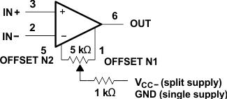
 Input Offset Voltage Null Circuit