SLOS183E February   1997  â€“ July 2025 TLE2141 , TLE2141A , TLE2142 , TLE2142A , TLE2142AM , TLE2142AM-D , TLE2142M , TLE2142M-D , TLE2144 , TLE2144A , TLE2144AM , TLE2144M , TLE2144M-D

PRODUCTION DATA  

  1.   1
  2. 1Features
  3. 2Applications
  4. 3Description
  5. 4Pin Configuration and Functions
  6. 5Specifications
    1. 5.1  Absolute Maximum Ratings
    2. 5.2  Recommended Operating Conditions
    3. 5.3  TLE2141C Electrical Characteristics
    4. 5.4  TLE2141C Operating Characteristics, VCC = 5V , TA = 25°C
    5. 5.5  TLE2141C Electrical Characteristics
    6. 5.6  TLE2141C Operating Characteristics, VCC± = ±15V , TA = 25°C
    7. 5.7  TLE2142C Electrical Characteristics
    8. 5.8  TLE2142C Operating Characteristics, VCC = 5V , TA = 25°C
    9. 5.9  TLE2142C Electrical Characteristics
    10. 5.10 TLE2142C Operating Characteristics, VCC± = ±15V , TA = 25°C
    11. 5.11 TLE2144C Electrical Characteristics
    12. 5.12 TLE2144C Operating Characteristics, VCC = 5V , TA = 25°C
    13. 5.13 TLE2144C Electrical Characteristics
    14. 5.14 TLE2144C Operating Characteristics, VCC± = ±15V , TA = 25°C
    15. 5.15 TLE2141I Electrical Characteristics
    16. 5.16 TLE2141I Operating Characteristics, VCC = 5V , TA = 25°C
    17. 5.17 TLE2141I Electrical Characteristics
    18. 5.18 TLE2141I Operating Characteristics, VCC± = ±15V , TA = 25°C
    19. 5.19 TLE2142I Electrical Characteristics
    20. 5.20 TLE2142I Operating Characteristics, VCC = 5V , TA = 25°C
    21. 5.21 TLE2142I Electrical Characteristics
    22. 5.22 TLE2142I Operating Characteristics, VCC± = ±15V , TA = 25°C
    23. 5.23 TLE2144I Electrical Characteristics
    24. 5.24 TLE2144C Operating Characteristics, VCC = 5V , TA = 25°C
    25. 5.25 TLE2144I Electrical Characteristics
    26. 5.26 TLE2144I Operating Characteristics, VCC± = ±15V , TA = 25°C
    27. 5.27 TLE2144I Electrical Characteristics
    28. 5.28 TLE2141M Operating Characteristics, VCC = 5V , TA = 25°C
    29. 5.29 TLE2141M Electrical Characteristics
    30. 5.30 TLE2141M Operating Characteristics, VCC± = ±15V , TA = 25°C
    31. 5.31 TLE2142M Electrical Characteristics
    32. 5.32 TLE2142M Operating Characteristics, VCC = 5V , TA = 25°C
    33. 5.33 TLE2142M Electrical Characteristics
    34. 5.34 TLE2142M Operating Characteristics, VCC± = ±15V , TA = 25°C
    35. 5.35 TLE2144M Electrical Characteristics
    36. 5.36 TLE2144M Operating Characteristics
    37. 5.37 TLE2144M Electrical Characteristics
    38. 5.38 TLE2144M Operating Characteristics
    39. 5.39 TLE2141Y Electrical Characteristics
    40. 5.40 TLE2142Y Electrical Characteristics
    41. 5.41 TLE2144Y Electrical Characteristics
    42. 5.42 Typical Characteristics
  7. 6Detailed Description
    1. 6.1 Overview
  8. 7Device and Documentation Support
    1. 7.1 Receiving Notification of Documentation Updates
    2. 7.2 Support Resources
    3. 7.3 Trademarks
    4. 7.4 Electrostatic Discharge Caution
    5. 7.5 Glossary
  9. 8Revision History
  10. 9Mechanical, Packaging, and Orderable Information

Package Options

Mechanical Data (Package|Pins)
Thermal pad, mechanical data (Package|Pins)
Orderable Information

Typical Characteristics

Table of Graphs
FIGURE
VIO Input offset voltage Distribution 1, 2, 3
IIO Input offset current vs Free-air temperature 4
IIB Input bias current vs Common-mode input voltage 5
vs Free-air temperature 6
VOM+ Maximum positive peak output voltage vs Supply voltage 7
vs Free-air temperature 8
vs Output current 9
vs Settling time 11
VOM− Maximum negative peak output voltage vs Supply voltage 7
vs Free-air temperature 8
vs Output current 10
vs Settling time 11
VO(PP) Maximum peak-to-peak output voltage vs Frequency 12
VOH High-level output voltage vs Output current 13
VOL Low-level output voltage vs Output current 14
AVD Large-signal differential voltage amplification vs Frequency 15
vs Free-air temperature 16
Phase shift vs Frequency 15
zo Closed-loop output impedance vs Frequency 17
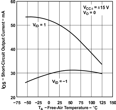
IOS Short-circuit output current vs Free-air temperature 18
CMRR Common-mode rejection ratio vs Frequency 19
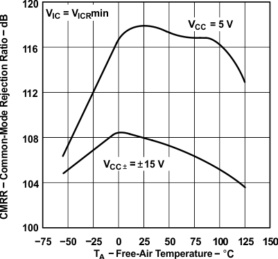
vs Free-air temperature 20
kSVR Supply-voltage rejection ratio vs Frequency 21
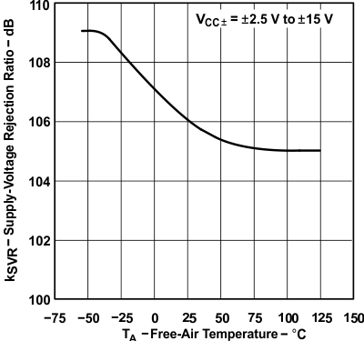
vs Free-air temperature 22
vs Supply voltage 23
ICC Supply current vs Free-air temperature 24
Vn Equivalent input noise voltage vs Frequency 25
Vn Input noise voltage Over a 10-second period 26
In Noise current vs Frequency 27
THD + N Total harmonic distortion plus noise vs Frequency 28
SR Slew rate vs Free-air temperature 29
vs Load capacitance 30
Pulse response Noninverting large signal vs Time 31
Inverting large signal vs Time 32
Small signal vs Time 33
B1 Unity-gain bandwidth vs Load capacitance 34
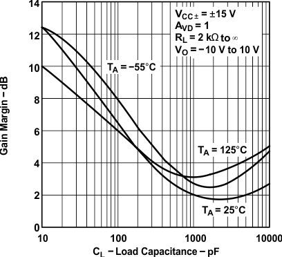
Gain margin vs Load capacitance 35
φm Phase margin vs Load capacitance 36
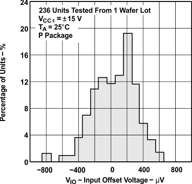
TLE2141 TLE2141A TLE2142 TLE2142A TLE2142AM TLE2142AM-D TLE2142M TLE2142M-D TLE2144 TLE2144A TLE2144AM TLE2144M TLE2144M-D TLE2141 Distribution of Input Offset
                        VoltageFigure 5-1 TLE2141 Distribution of Input Offset Voltage
TLE2141 TLE2141A TLE2142 TLE2142A TLE2142AM TLE2142AM-D TLE2142M TLE2142M-D TLE2144 TLE2144A TLE2144AM TLE2144M TLE2144M-D TLE2144 Distribution of Input Offset
                        Voltage
TEST To remove kickback errors


Figure 5-3 TLE2144 Distribution of Input Offset Voltage
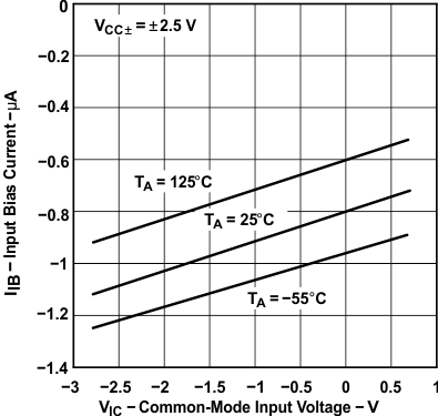
TLE2141 TLE2141A TLE2142 TLE2142A TLE2142AM TLE2142AM-D TLE2142M TLE2142M-D TLE2144 TLE2144A TLE2144AM TLE2144M TLE2144M-D Input Bias Current(1) vs
                        Common-Mode Input Voltage
1. Data at high and low temperatures are applicable only within the rated operating free-air temperature ranges of the various devices.
Figure 5-5 Input Bias Current(1) vs Common-Mode Input Voltage
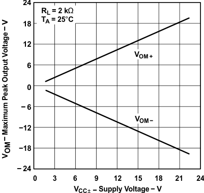
TLE2141 TLE2141A TLE2142 TLE2142A TLE2142AM TLE2142AM-D TLE2142M TLE2142M-D TLE2144 TLE2144A TLE2144AM TLE2144M TLE2144M-D Maximum Peak Output Voltage vs Supply
                        VoltageFigure 5-7 Maximum Peak Output Voltage vs Supply Voltage
TLE2141 TLE2141A TLE2142 TLE2142A TLE2142AM TLE2142AM-D TLE2142M TLE2142M-D TLE2144 TLE2144A TLE2144AM TLE2144M TLE2144M-D Maximum Positive Peak Output
                            Voltage(1) vs Output Current
1. Data at high and low temperatures are applicable only within the rated operating free-air temperature ranges of the various devices.
Figure 5-9 Maximum Positive Peak Output Voltage(1) vs Output Current
TLE2141 TLE2141A TLE2142 TLE2142A TLE2142AM TLE2142AM-D TLE2142M TLE2142M-D TLE2144 TLE2144A TLE2144AM TLE2144M TLE2144M-D Maximum Peak Output Voltage vs Settling
                        Time


Figure 5-11 Maximum Peak Output Voltage vs Settling Time
TLE2141 TLE2141A TLE2142 TLE2142A TLE2142AM TLE2142AM-D TLE2142M TLE2142M-D TLE2144 TLE2144A TLE2144AM TLE2144M TLE2144M-D High-Level Output Voltage(1) vs
                        Output Current
1. Data at high and low temperatures are applicable only within the rated operating free-air temperature ranges of the various devices.
Figure 5-13 High-Level Output Voltage(1) vs Output Current
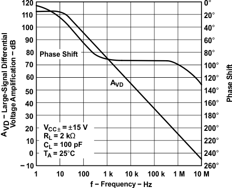
TLE2141 TLE2141A TLE2142 TLE2142A TLE2142AM TLE2142AM-D TLE2142M TLE2142M-D TLE2144 TLE2144A TLE2144AM TLE2144M TLE2144M-D Large-Signal Differential Voltage
                        Amplification and Phase Shift vs Frequency


Figure 5-15 Large-Signal Differential Voltage Amplification and Phase Shift vs Frequency
TLE2141 TLE2141A TLE2142 TLE2142A TLE2142AM TLE2142AM-D TLE2142M TLE2142M-D TLE2144 TLE2144A TLE2144AM TLE2144M TLE2144M-D TLE2142 Distribution of Input Offset
                        VoltageFigure 5-2 TLE2142 Distribution of Input Offset Voltage
TLE2141 TLE2141A TLE2142 TLE2142A TLE2142AM TLE2142AM-D TLE2142M TLE2142M-D TLE2144 TLE2144A TLE2144AM TLE2144M TLE2144M-D Input Offset Current(1) Offset
                        Voltage
1. Data at high and low temperatures are applicable only within the rated operating free-air temperature ranges of the various devices.
Figure 5-4 Input Offset Current(1) Offset Voltage
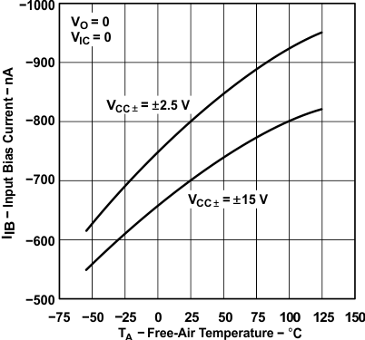
TLE2141 TLE2141A TLE2142 TLE2142A TLE2142AM TLE2142AM-D TLE2142M TLE2142M-D TLE2144 TLE2144A TLE2144AM TLE2144M TLE2144M-D Input Bias Current(1) vs Free-Air
                        Temperature
1. Data at high and low temperatures are applicable only within the rated operating free-air temperature ranges of the various devices.
Figure 5-6 Input Bias Current(1) vs Free-Air Temperature
TLE2141 TLE2141A TLE2142 TLE2142A TLE2142AM TLE2142AM-D TLE2142M TLE2142M-D TLE2144 TLE2144A TLE2144AM TLE2144M TLE2144M-D Maximum Peak Output Voltage vs Free-Air
                        TemperatureFigure 5-8 Maximum Peak Output Voltage vs Free-Air Temperature
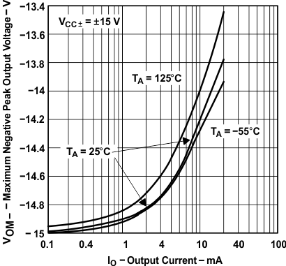
TLE2141 TLE2141A TLE2142 TLE2142A TLE2142AM TLE2142AM-D TLE2142M TLE2142M-D TLE2144 TLE2144A TLE2144AM TLE2144M TLE2144M-D Maximum Negative Peak Output
                            Voltage(1) vs Output Current
1. Data at high and low temperatures are applicable only within the rated operating free-air temperature ranges of the various devices.
Figure 5-10 Maximum Negative Peak Output Voltage(1) vs Output Current
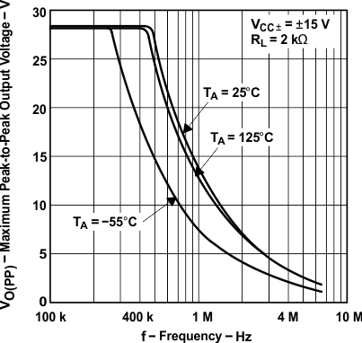
TLE2141 TLE2141A TLE2142 TLE2142A TLE2142AM TLE2142AM-D TLE2142M TLE2142M-D TLE2144 TLE2144A TLE2144AM TLE2144M TLE2144M-D Maximum Peak-to-Peak Output
                            Voltage(1) vs Frequency
1. Data at high and low temperatures are applicable only within the rated operating free-air temperature ranges of the various devices.
Figure 5-12 Maximum Peak-to-Peak Output Voltage(1) vs Frequency
TLE2141 TLE2141A TLE2142 TLE2142A TLE2142AM TLE2142AM-D TLE2142M TLE2142M-D TLE2144 TLE2144A TLE2144AM TLE2144M TLE2144M-D Low-Level Output Voltage(1) vs
                        Output Current
1. Data at high and low temperatures are applicable only within the rated operating free-air temperature ranges of the various devices.
Figure 5-14 Low-Level Output Voltage(1) vs Output Current
TLE2141 TLE2141A TLE2142 TLE2142A TLE2142AM TLE2142AM-D TLE2142M TLE2142M-D TLE2144 TLE2144A TLE2144AM TLE2144M TLE2144M-D Large-Signal Differential Voltage
                            Amplification(1) vs Free-Air Temperature
1. Data at high and low temperatures are applicable only within the rated operating free-air temperature ranges of the various devices.
Figure 5-16 Large-Signal Differential Voltage Amplification(1) vs Free-Air Temperature
TLE2141 TLE2141A TLE2142 TLE2142A TLE2142AM TLE2142AM-D TLE2142M TLE2142M-D TLE2144 TLE2144A TLE2144AM TLE2144M TLE2144M-D Closed-Loop Output Impedance vs
                        Frequency


Figure 5-17 Closed-Loop Output Impedance vs Frequency
TLE2141 TLE2141A TLE2142 TLE2142A TLE2142AM TLE2142AM-D TLE2142M TLE2142M-D TLE2144 TLE2144A TLE2144AM TLE2144M TLE2144M-D Common-Mode Rejection Ratio vs
                        Frequency


Figure 5-19 Common-Mode Rejection Ratio vs Frequency
TLE2141 TLE2141A TLE2142 TLE2142A TLE2142AM TLE2142AM-D TLE2142M TLE2142M-D TLE2144 TLE2144A TLE2144AM TLE2144M TLE2144M-D Supply-Voltage Rejection Ratio vs
                        Frequency


Figure 5-21 Supply-Voltage Rejection Ratio vs Frequency
TLE2141 TLE2141A TLE2142 TLE2142A TLE2142AM TLE2142AM-D TLE2142M TLE2142M-D TLE2144 TLE2144A TLE2144AM TLE2144M TLE2144M-D Supply Current(1) vs Supply
                        Voltage
1. Data at high and low temperatures are applicable only within the rated operating free-air temperature ranges of the various devices.
Figure 5-23 Supply Current(1) vs Supply Voltage
TLE2141 TLE2141A TLE2142 TLE2142A TLE2142AM TLE2142AM-D TLE2142M TLE2142M-D TLE2144 TLE2144A TLE2144AM TLE2144M TLE2144M-D Equivalent Input Noise Voltage(1)
                        vs Frequency
1. Data at high and low temperatures are applicable only within the rated operating free-air temperature ranges of the various devices.
Figure 5-25 Equivalent Input Noise Voltage(1) vs Frequency
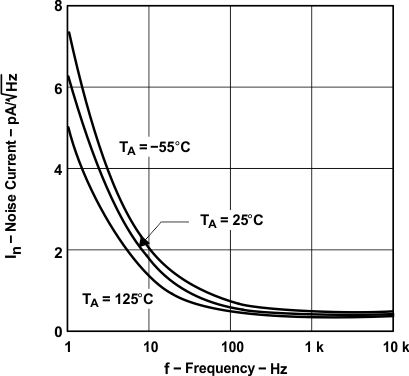
TLE2141 TLE2141A TLE2142 TLE2142A TLE2142AM TLE2142AM-D TLE2142M TLE2142M-D TLE2144 TLE2144A TLE2144AM TLE2144M TLE2144M-D Noise Current(1) vs
                        Frequency
1. Data at high and low temperatures are applicable only within the rated operating free-air temperature ranges of the various devices.
Figure 5-27 Noise Current(1) vs Frequency
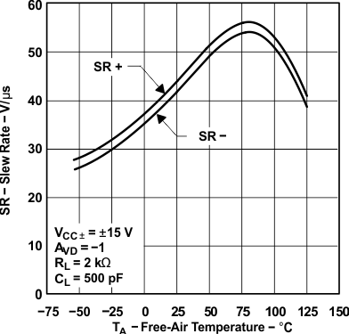
TLE2141 TLE2141A TLE2142 TLE2142A TLE2142AM TLE2142AM-D TLE2142M TLE2142M-D TLE2144 TLE2144A TLE2144AM TLE2144M TLE2144M-D Slew Rate(1) vs Free-Air
                        Temperature
1. Data at high and low temperatures are applicable only within the rated operating free-air temperature ranges of the various devices.
Figure 5-29 Slew Rate(1) vs Free-Air Temperature
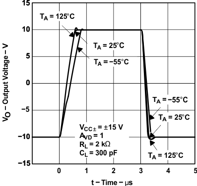
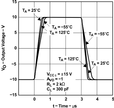
TLE2141 TLE2141A TLE2142 TLE2142A TLE2142AM TLE2142AM-D TLE2142M TLE2142M-D TLE2144 TLE2144A TLE2144AM TLE2144M TLE2144M-D Noninverting Large-Signal Pulse
                            Response(1)
1. Data at high and low temperatures are applicable only within the rated operating free-air temperature ranges of the various devices.
Figure 5-31 Noninverting Large-Signal Pulse Response(1)
TLE2141 TLE2141A TLE2142 TLE2142A TLE2142AM TLE2142AM-D TLE2142M TLE2142M-D TLE2144 TLE2144A TLE2144AM TLE2144M TLE2144M-D Small-Signal Pulse Response


Figure 5-33 Small-Signal Pulse Response
TLE2141 TLE2141A TLE2142 TLE2142A TLE2142AM TLE2142AM-D TLE2142M TLE2142M-D TLE2144 TLE2144A TLE2144AM TLE2144M TLE2144M-D Gain Margin vs Load Capacitance


Figure 5-35 Gain Margin vs Load Capacitance
TLE2141 TLE2141A TLE2142 TLE2142A TLE2142AM TLE2142AM-D TLE2142M TLE2142M-D TLE2144 TLE2144A TLE2144AM TLE2144M TLE2144M-D Short-Circuit Output Current(1) vs
                        Free-Air Temperature
1. Data at high and low temperatures are applicable only within the rated operating free-air temperature ranges of the various devices.
Figure 5-18 Short-Circuit Output Current(1) vs Free-Air Temperature
TLE2141 TLE2141A TLE2142 TLE2142A TLE2142AM TLE2142AM-D TLE2142M TLE2142M-D TLE2144 TLE2144A TLE2144AM TLE2144M TLE2144M-D Common-Mode Rejection Ratio(1) vs
                        Free-Air Temperature
1. Data at high and low temperatures are applicable only within the rated operating free-air temperature ranges of the various devices.
Figure 5-20 Common-Mode Rejection Ratio(1) vs Free-Air Temperature
TLE2141 TLE2141A TLE2142 TLE2142A TLE2142AM TLE2142AM-D TLE2142M TLE2142M-D TLE2144 TLE2144A TLE2144AM TLE2144M TLE2144M-D Supply-Voltage Rejection Ratio(1)
                        vs Free-Air Temperature
1. Data at high and low temperatures are applicable only within the rated operating free-air temperature ranges of the various devices.
Figure 5-22 Supply-Voltage Rejection Ratio(1) vs Free-Air Temperature
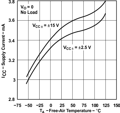
TLE2141 TLE2141A TLE2142 TLE2142A TLE2142AM TLE2142AM-D TLE2142M TLE2142M-D TLE2144 TLE2144A TLE2144AM TLE2144M TLE2144M-D Supply Current(1) vs Free-Air
                        Temperature
1. Data at high and low temperatures are applicable only within the rated operating free-air temperature ranges of the various devices.
Figure 5-24 Supply Current(1) vs Free-Air Temperature
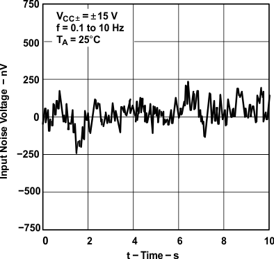
TLE2141 TLE2141A TLE2142 TLE2142A TLE2142AM TLE2142AM-D TLE2142M TLE2142M-D TLE2144 TLE2144A TLE2144AM TLE2144M TLE2144M-D Input Noise Voltage Over a 10-Second
                        Period


Figure 5-26 Input Noise Voltage Over a 10-Second Period
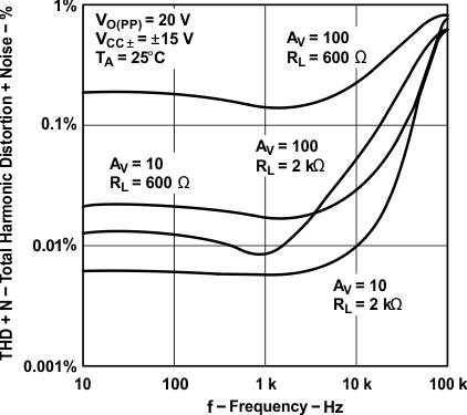
TLE2141 TLE2141A TLE2142 TLE2142A TLE2142AM TLE2142AM-D TLE2142M TLE2142M-D TLE2144 TLE2144A TLE2144AM TLE2144M TLE2144M-D Total Harmonic Distortion Plus Noise vs
                        Frequency


Figure 5-28 Total Harmonic Distortion Plus Noise vs Frequency
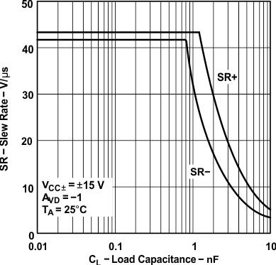
TLE2141 TLE2141A TLE2142 TLE2142A TLE2142AM TLE2142AM-D TLE2142M TLE2142M-D TLE2144 TLE2144A TLE2144AM TLE2144M TLE2144M-D Slew Rate vs Load Capacitance


Figure 5-30 Slew Rate vs Load Capacitance
TLE2141 TLE2141A TLE2142 TLE2142A TLE2142AM TLE2142AM-D TLE2142M TLE2142M-D TLE2144 TLE2144A TLE2144AM TLE2144M TLE2144M-D Inverting Large-Signal Pulse
                            Response(1)
1. Data at high and low temperatures are applicable only within the rated operating free-air temperature ranges of the various devices.
Figure 5-32 Inverting Large-Signal Pulse Response(1)
TLE2141 TLE2141A TLE2142 TLE2142A TLE2142AM TLE2142AM-D TLE2142M TLE2142M-D TLE2144 TLE2144A TLE2144AM TLE2144M TLE2144M-D Unity-Gain Bandwidth(1) vs Load
                        Capacitance
1. Data at high and low temperatures are applicable only within the rated operating free-air temperature ranges of the various devices.
Figure 5-34 Unity-Gain Bandwidth(1) vs Load Capacitance
TLE2141 TLE2141A TLE2142 TLE2142A TLE2142AM TLE2142AM-D TLE2142M TLE2142M-D TLE2144 TLE2144A TLE2144AM TLE2144M TLE2144M-D Phase Margin(1)
                        vs Load Capacitance
1. Data at high and low temperatures are applicable only within the rated operating free-air temperature ranges of the various devices.
Figure 5-36 Phase Margin(1) vs Load Capacitance