SLVSDO6D August   2017  – December 2024 TPS1H000-Q1

PRODUCTION DATA  

  1.   1
  2. Features
  3. Applications
  4. Description
  5. Pin Configuration and Functions
  6. Specifications
    1. 5.1 Absolute Maximum Ratings
    2. 5.2 ESD Ratings
    3. 5.3 Recommended Operating Conditions
    4. 5.4 Thermal Information
    5. 5.5 Electrical Characteristics
    6. 5.6 Switching Characteristics
    7. 5.7 Typical Characteristics
  7. Detailed Description
    1. 6.1 Overview
    2. 6.2 Functional Block Diagram
    3. 6.3 Feature Description
      1. 6.3.1 Current Limit
      2. 6.3.2 DELAY Pin Configuration
        1. 6.3.2.1 Holding Mode
        2. 6.3.2.2 Latch-Off Mode
        3. 6.3.2.3 Auto-Retry Mode
      3. 6.3.3 Standalone Operation
      4. 6.3.4 Fault Truth Table
      5. 6.3.5 Full Diagnostics
        1. 6.3.5.1 Short-to-GND and Overload Detection
        2. 6.3.5.2 Open-Load Detection
          1. 6.3.5.2.1 Output On
          2. 6.3.5.2.2 Output Off
        3. 6.3.5.3 Short-to-Battery Detection
        4. 6.3.5.4 Thermal Fault Detection
          1. 6.3.5.4.1 Thermal Shutdown
          2. 6.3.5.4.2 Thermal Swing
          3. 6.3.5.4.3 Fault Report Holding
      6. 6.3.6 Full Protections
        1. 6.3.6.1 UVLO Protection
        2. 6.3.6.2 Inductive Load Switching Off Clamp
        3. 6.3.6.3 Loss-of-GND Protection
        4. 6.3.6.4 Loss-of-Power-Supply Protection
        5. 6.3.6.5 Reverse-Current Protection
        6. 6.3.6.6 MCU I/O Protection
    4. 6.4 Device Functional Modes
      1. 6.4.1 Working Modes
        1. 6.4.1.1 Normal Mode
        2. 6.4.1.2 Standby Mode
        3. 6.4.1.3 Standby Mode With Diagnostics
  8. Application and Implementation
    1. 7.1 Application Information
    2. 7.2 Typical Application
      1. 7.2.1 Design Requirements
      2. 7.2.2 Detailed Design Procedure
      3. 7.2.3 Application Curves
    3. 7.3 Power Supply Recommendations
    4. 7.4 Layout
      1. 7.4.1 Layout Guidelines
      2. 7.4.2 Layout Example
  9. Device and Documentation Support
    1. 8.1 Receiving Notification of Documentation Updates
    2. 8.2 Support Resources
    3. 8.3 Trademarks
    4. 8.4 Electrostatic Discharge Caution
    5. 8.5 Glossary
  10. Revision History
  11. 10Mechanical, Packaging, and Orderable Information

Package Options

Mechanical Data (Package|Pins)
Thermal pad, mechanical data (Package|Pins)
Orderable Information

Latch-Off Mode

Latch-off mode is active when the DELAY pin connects to GND through a capacitor. When hitting a current limit, the output current holds at the setting current, but latches off after a preset DELAY time (tdl1+ tdl2). tdl1 is the default delay time, tdl2 is a configurable delay time set by a capacitor. The output stays latched off regardless of whether the current limit is removed. The output recovers only when IN is toggling.

tdl2 can be calculated by Equation 2. The Idl(chg)is the device charging current in latch-off mode, Vdl(ref) is the internal reference voltage in latch off mode, tdl2 is the user-setting delay time, and CDELAY is the capacitor connected on the DELAY pin.

Equation 2. TPS1H000-Q1
TPS1H000-Q1 Latch-Off-Mode Connection
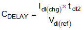
Figure 6-4 Latch-Off-Mode Connection
TPS1H000-Q1 Latch-Off-Mode ExampleFigure 6-5 Latch-Off-Mode Example