SLVSGK4A November 2021 – June 2022 TPS22953-Q1 , TPS22954-Q1
PRODUCTION DATA
- 1 Features
- 2 Applications
- 3 Description
- 4 Revision History
- 5 Device Comparison Table
- 6 Pin Configuration and Functions
-
7 Specifications
- 7.1 Absolute Maximum Ratings
- 7.2 ESD Ratings
- Recommended Operating Conditions
- 7.3 Thermal Information
- 7.4 Electrical Characteristics
- 7.5 Electrical Characteristics – VBIAS = 5 V
- 7.6 Electrical Characteristics – VBIAS = 3.3 V
- 7.7 Electrical Characteristics – VBIAS = 2.5 V
- 7.8 Switching Characteristics – CT = 1000 pF
- 7.9 Switching Characteristics – CT = 0 pF
- 7.10 Typical DC Characteristics
- 7.11 Typical Switching Characteristics
- 8 Parameter Measurement Information
-
9 Detailed Description
- 9.1 Overview
- 9.2 Functional Block Diagram
- 9.3
Feature Description
- 9.3.1 On and Off Control (EN Pin)
- 9.3.2 Voltage Monitoring (SNS Pin)
- 9.3.3 Power Good (PG Pin)
- 9.3.4 Supervisor Fault Detection and Automatic Restart
- 9.3.5 Manual Restart
- 9.3.6 Thermal Shutdown
- 9.3.7 Reverse Current Blocking (TPS22953-Q1 Only)
- 9.3.8 Quick Output Discharge (QOD) (TPS22954-Q1 Only)
- 9.3.9 VIN and VBIAS Voltage Range
- 9.3.10 Adjustable Rise Time (CT Pin)
- 9.3.11 Power Sequencing
- 9.4 Device Functional Modes
- 10Application and Implementation
- 11Power Supply Recommendations
- 12Layout
- 13Device and Documentation Support
- 14Mechanical, Packaging, and Orderable Information
Package Options
Mechanical Data (Package|Pins)
- DQC|10
Thermal pad, mechanical data (Package|Pins)
- DQC|10
Orderable Information
10.1.6 Break-Before-Make Power MUX (TPS22953-Q1 Only)
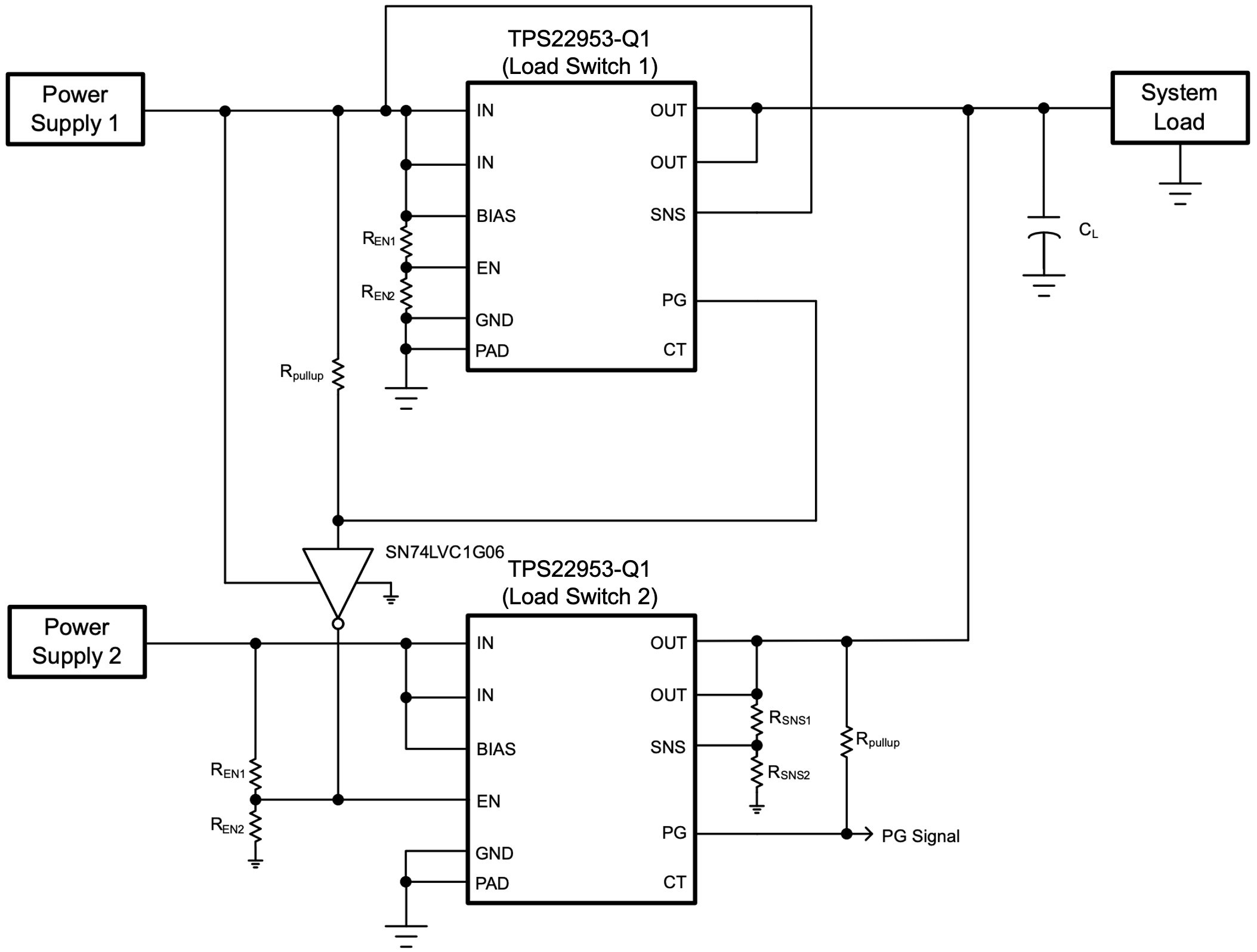
The reverse current blocking feature of the TPS22953-Q1 makes it suitable for power multiplexing (MUXing) between two power supplies with different voltages. The SNS and PG pin can be configured to implement break-before-make logic. The circuit in Figure 10-4 shows how the detection of power supply 1 can be used to disable the load switch for power supply 2. By tying the SNS of Load Switch 1 directly to the input, its PG pin is pulled up as soon as the device is enabled.
 Figure 10-4 Break-Before-Make Power MUX Schematic
The break-before-make logic ensures that power supply 2 is completely disconnected before power supply 1 is connected. This approach provides very robust reverse current blocking. However, in most cases, this aproach also results in a dip in the output voltage when switching between supplies.
The amount of voltage dip depends on the loading, the output capacitance, and the turn-on delay of the load switch. In this application, leaving the CT pin open results in the shortest turn-on delay and minimizes the output voltage dip.
Table 10-1 summarizes the logic of the PG Signal for Figure 10-4.
| PG Signal | Indication |
|---|---|
| H | Power supply 1 not present. System powered from power supply 2. |
| L | Power supply 1 present. System powered from power supply 1. |