SLVSCD6A December   2015  – January 2021 TPS62097

PRODUCTION DATA  

  1. Features
  2. Applications
  3. Description
  4. Revision History
  5. Device Options
  6. Pin Configuration and Functions
  7. Specifications
    1. 7.1 Absolute Maximum Ratings
    2. 7.2 ESD Ratings
    3. 7.3 Recommend Operating Conditions
    4. 7.4 Thermal Information
    5. 7.5 Electrical Characteristics
    6. 7.6 Typical Characteristics
  8. Detailed Description
    1. 8.1 Overview
    2. 8.2 Functional Block Diagram
    3. 8.3 Feature Description
      1. 8.3.1 100% Duty Cycle Mode
      2. 8.3.2 Switch Current Limit and Hiccup Short Circuit Protection
      3. 8.3.3 Undervoltage Lockout (UVLO)
      4. 8.3.4 Thermal Shutdown
    4. 8.4 Device Function Modes
      1. 8.4.1 Enable and Disable (EN)
      2. 8.4.2 Power Save Mode and Forced PWM Mode (MODE)
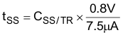
      3. 8.4.3 Soft Start-up (SS/TR)
      4. 8.4.4 Voltage Tracking (SS/TR)
      5. 8.4.5 Power Good (PG)
  9. Application and Implementation
    1. 9.1 Application Information
    2. 9.2 1.2-V Output Application
      1. 9.2.1 Design Requirements
      2. 9.2.2 Detailed Design Procedure
        1. 9.2.2.1 Setting the Output Voltage
        2. 9.2.2.2 Output Filter Design
        3. 9.2.2.3 Inductor Selection
        4. 9.2.2.4 Capacitor Selection
      3. 9.2.3 Application Performance Curves
      4. 9.2.4 Coincidental Voltage Tracking
        1. 9.2.4.1 Design Requirements
        2. 9.2.4.2 Detailed Design Procedure
        3. 9.2.4.3 Application Performance Curve
      5. 9.2.5 Switching Frequency Selection
        1. 9.2.5.1 Design Requirements
        2. 9.2.5.2 Detailed Design Procedure
        3. 9.2.5.3 Application Performance Curves
  10. 10Power Supply Recommendations
  11. 11Layout
    1. 11.1 Layout Guidelines
    2. 11.2 Layout Example
      1. 11.2.1 Thermal Information
  12. 12Device and Documentation Support
    1. 12.1 Device Support
      1. 12.1.1 Third-Party Products Disclaimer
    2. 12.2 Support Resources
    3. 12.3 Receiving Notification of Documentation Updates
    4. 12.4 Trademarks
    5. 12.5 Electrostatic Discharge Caution
    6. 12.6 Glossary
  13. 13Mechanical, Packaging, and Orderable Information

Package Options

Mechanical Data (Package|Pins)
Thermal pad, mechanical data (Package|Pins)
Orderable Information

Soft Start-up (SS/TR)

The TPS62097 programs its output voltage ramp rate with the SS/TR pin. Connecting an external capacitor to SS/TR enables output soft start-up to reduce inrush current from the input supply. The device charges the capacitor voltage to the input supply voltage with a constant current of typically 7.5 μA. The FB pin voltage follows the SS/TR pin voltage until the internal reference voltage of 0.8 V is reached. The soft start-up time is calculated using Equation 3. Keep the SS/TR pin floating to set the minimum start-up time.

Equation 3. GUID-3DA50763-D01C-4B58-AF9D-EBC272F2E2EC-low.gif

An active pulldown circuit is connected to the SS/TR pin. It discharges the external soft start-up capacitor in case of disable, UVLO, thermal shutdown, and HICCUP short circuit protection.