SBOS394E November 2007 – July 2019 VCA824
PRODUCTION DATA.
- 1 Features
- 2 Applications
- 3 Description
- 4 Revision History
- 5 Device Comparison Table
- 6 Pin Configuration and Functions
-
7 Specifications
- 7.1 Absolute Maximum Ratings
- 7.2 ESD Ratings
- 7.3 Recommended Operating Conditions
- 7.4 Thermal Information
- 7.5 Electrical Characteristics: VS = ±5 V
- 7.6 Typical Characteristics: VS = ±5 V, AVMAX = 2 V/V
- 7.7 Typical Characteristics: VS = ±5 V, AVMAX = 10 V/V
- 7.8 Typical Characteristics: VS = ±5 V, AVMAX = 40 V/V
- 8 Detailed Description
- 9 Application and Implementation
- 10Power Supply Recommendations
- 11Layout
- 12Device and Documentation Support
- 13Mechanical, Packaging, and Orderable Information
Package Options
Mechanical Data (Package|Pins)
Thermal pad, mechanical data (Package|Pins)
Orderable Information
9.1.2 Differential Equalizer
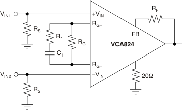
If the application requires frequency shaping (the transition from one gain to another), the VCA824 can be used advantageously because its architecture allows the application to isolate the input from the gain setting elements. Figure 70 shows an implementation of such a configuration. The transfer function is shown in Equation 5.

 Figure 70. Differential Equalizer
 This transfer function has one pole, P1 (located at RGC1), and one zero, Z1 (located at R1C1). When equalizing an RC load, RL and CL, compensate the pole added by the load located at RLCL with the zero Z1. Knowing RL, CL, and RG allows the user to select C1 as a first step and then calculate R1. Using RL = 75-Ω, CL = 100pF and wanting the VCA824 to operate at a gain of 2 V/V, which gives RF = RG = 453-kΩ, allows the user to select
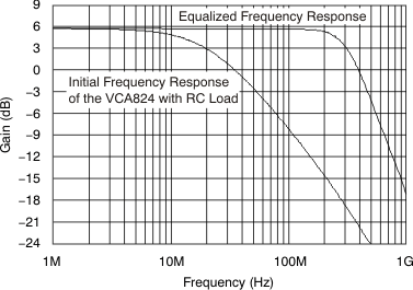
C1 = 15.5 pF to ensure a positive value for the resistor R1. With all these values known, to achieve greater than 300 MHz bandwidth, R1 can be calculated to be 20-Ω. Figure 71 shows the frequency response for both the initial, unequalized frequency response and the resulting equalized frequency response.
 Figure 71. Differential Equalization of an RC Load