SBOS394E November 2007 – July 2019 VCA824
PRODUCTION DATA.
- 1 Features
- 2 Applications
- 3 Description
- 4 Revision History
- 5 Device Comparison Table
- 6 Pin Configuration and Functions
-
7 Specifications
- 7.1 Absolute Maximum Ratings
- 7.2 ESD Ratings
- 7.3 Recommended Operating Conditions
- 7.4 Thermal Information
- 7.5 Electrical Characteristics: VS = ±5 V
- 7.6 Typical Characteristics: VS = ±5 V, AVMAX = 2 V/V
- 7.7 Typical Characteristics: VS = ±5 V, AVMAX = 10 V/V
- 7.8 Typical Characteristics: VS = ±5 V, AVMAX = 40 V/V
- 8 Detailed Description
- 9 Application and Implementation
- 10Power Supply Recommendations
- 11Layout
- 12Device and Documentation Support
- 13Mechanical, Packaging, and Orderable Information
Package Options
Mechanical Data (Package|Pins)
Thermal pad, mechanical data (Package|Pins)
- D|14
Orderable Information
7.7 Typical Characteristics: VS = ±5 V, AVMAX = 10 V/V
At TA = 25°C, RL = 100 Ω, RF = 402 Ω, RG = 80 Ω, VG = 1 V, and VIN = single-ended input on +VIN with –VIN at ground, unless otherwise noted.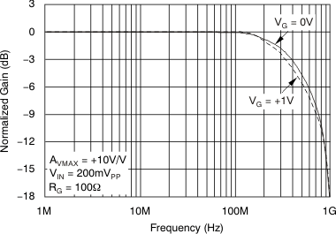 Figure 23. Small-Signal Frequency Response
 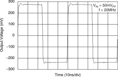 Figure 25. Small-Signal Pulse Response
 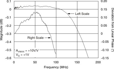 Figure 27. Gain Flatness, Deviation from Linear Phase
 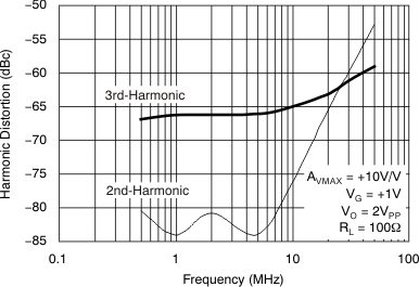 Figure 29. Harmonic Distortion vs Frequency
 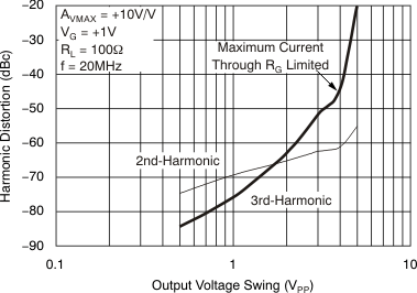 Figure 31. Harmonic Distortion vs Output Voltage
 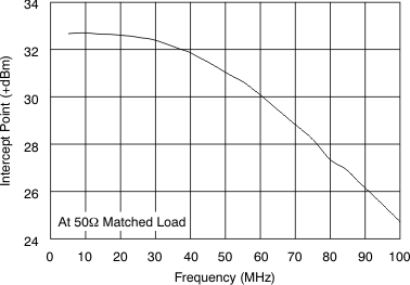 Figure 33. Two-Tone, 3rd-Order Intermodulation Intercept
 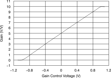 Figure 35. Gain vs Gain Control Voltage
 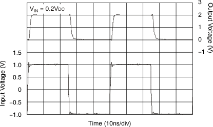 Figure 37. Gain Control Pulse Response
 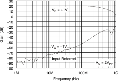 Figure 39. Fully-Attenuated Response
 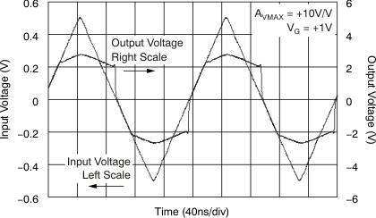 Figure 41. Output Limited Overdrive Recovery
 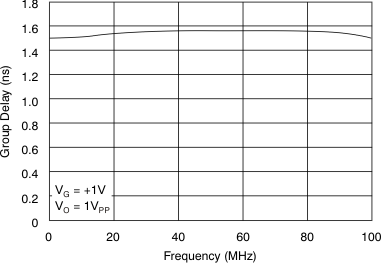 Figure 43. Group Delay vs Frequency
 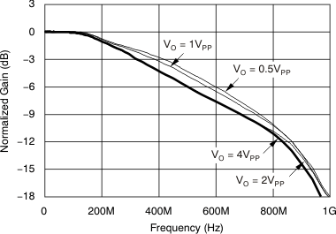 Figure 24. Large-Signal Frequency Response
 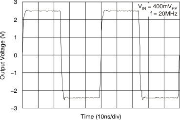 Figure 26. Large-Signal Pulse Response
 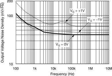 Figure 28. Output Voltage Noise Density
 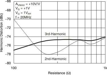 Figure 30. Harmonic Distortion vs Load Resistance
 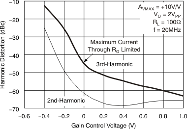 Figure 32. Harmonic Distortion vs Gain Control Voltage
 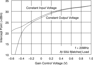 Figure 34. Two-Tone, 3rd-Order Intermodulation Intercept vs Gain Control Voltage
 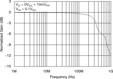 Figure 36. Gain Control Frequency Response
 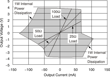 Figure 38. Output Voltage and Current Limitations
 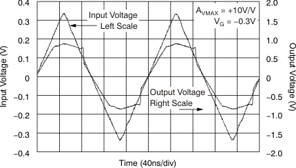 Figure 40. IRG Limited Overdrive Recovery
 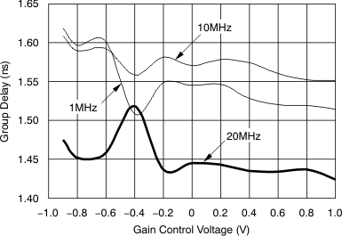 Figure 42. Group Delay vs Gain Control Voltage