SBOS394E November 2007 – July 2019 VCA824
PRODUCTION DATA.
- 1 Features
- 2 Applications
- 3 Description
- 4 Revision History
- 5 Device Comparison Table
- 6 Pin Configuration and Functions
-
7 Specifications
- 7.1 Absolute Maximum Ratings
- 7.2 ESD Ratings
- 7.3 Recommended Operating Conditions
- 7.4 Thermal Information
- 7.5 Electrical Characteristics: VS = ±5 V
- 7.6 Typical Characteristics: VS = ±5 V, AVMAX = 2 V/V
- 7.7 Typical Characteristics: VS = ±5 V, AVMAX = 10 V/V
- 7.8 Typical Characteristics: VS = ±5 V, AVMAX = 40 V/V
- 8 Detailed Description
- 9 Application and Implementation
- 10Power Supply Recommendations
- 11Layout
- 12Device and Documentation Support
- 13Mechanical, Packaging, and Orderable Information
Package Options
Mechanical Data (Package|Pins)
Thermal pad, mechanical data (Package|Pins)
- D|14
Orderable Information
9.1.5 Wideband Variable Gain Amplifier Operation
The VCA824 provides an exceptional combination of high output power capability with a wideband, greater than 40dB gain adjust range, linear in V/V variable gain amplifier. The VCA824 input stage places the transconductance element between two input buffers, using the output currents as the forward signal. As the differential input voltage rises, a signal current is generated through the gain element. This current is then mirrored and gained by a factor of two before reaching the multiplier. The other input of the multiplier is the voltage gain control pin, VG. Depending on the voltage present on VG, up to two times the gain current is provided to the transimpedance output stage. The transimpedance output stage is a current-feedback amplifier providing high output current capability and high slew rate, 2500 V/μs. This exceptional full-power performance comes at the price of relatively high quiescent current (36.5 mA), but low input voltage noise for this type of architecture (6 nV/√Hz).
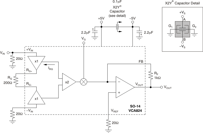
Figure 75 shows the dc-coupled, gain of 10 V/V, dual power-supply circuit used as the basis of Electrical Characteristics- Vs = ± 5 VElectrical Characteristics: VS = ±5 V and Typical Characteristics. For test purposes, the input impedance is set to 50-Ω with a resistor to ground and the output impedance is set to 50-Ω with a series output resistor. Voltage swings reported in Electrical Characteristics- VS = ± 5 V are taken directly at the input and output pins, while output power (dBm) is at the matched 50-Ω load. For the circuit in Figure 75, the total effective load is 100-Ω ∥ 1-kΩ. Note that for the 14-pin, SOIC package, there is a voltage reference pin, VREF (pin 9). For the 14-pin SOIC package, this pin must be connected to ground through a 20-Ω resistor to avoid possible oscillations of the output stage. In the 10-pin, MSOP package, this pin is internally connected and does not require such precaution. An X2Y® capacitor has been used for power-supply bypassing. The combination of low inductance, high resonance frequency, and integration of three capacitors in one package (two capacitors to ground and one across the supplies) enables the VCA824 to achieve the low second-harmonic distortion reported in Electrical Characteristics- VS = ± 5 V.
 Figure 75. DC-Coupled, AVMAX = 10 V/V, Bipolar Supply Specification and Test Circuit