SBOS394E November 2007 – July 2019 VCA824
PRODUCTION DATA.
- 1 Features
- 2 Applications
- 3 Description
- 4 Revision History
- 5 Device Comparison Table
- 6 Pin Configuration and Functions
-
7 Specifications
- 7.1 Absolute Maximum Ratings
- 7.2 ESD Ratings
- 7.3 Recommended Operating Conditions
- 7.4 Thermal Information
- 7.5 Electrical Characteristics: VS = ±5 V
- 7.6 Typical Characteristics: VS = ±5 V, AVMAX = 2 V/V
- 7.7 Typical Characteristics: VS = ±5 V, AVMAX = 10 V/V
- 7.8 Typical Characteristics: VS = ±5 V, AVMAX = 40 V/V
- 8 Detailed Description
- 9 Application and Implementation
- 10Power Supply Recommendations
- 11Layout
- 12Device and Documentation Support
- 13Mechanical, Packaging, and Orderable Information
Package Options
Mechanical Data (Package|Pins)
Thermal pad, mechanical data (Package|Pins)
Orderable Information
9.2 Typical Application
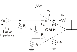
A four-quadrant multiplier can easily be implemented using the VCA824. By placing a resistor between FB and VIN, the transfer function depends upon both VIN and VG, as shown in Equation 10.
Equation 10. 

Setting R1 to equal RG, the term that depends only on VIN drops out of the equation, leaving only the term that depends on both VG and VIN. VOUT then follows Equation 11.
Equation 11. 

 Figure 76. Four-Quadrant Multiplier Circuit
 Figure 77 illustrates the behavior of this circuit. Keeping the input amplitude of a 1-MHz signal constant and varying the VG voltage (100 kHz, 2 VPP) gives the modulated output voltage shown in Figure 77.