JAJSPW8E march 2011 – february 2023 ADS4222 , ADS4225 , ADS4226 , ADS4242 , ADS4245 , ADS4246
PRODUCTION DATA
- 1 特長
- 2 アプリケーション
- 3 概要
- 4 Revision History
- 5 概要 (続き)
- 6 Pin Configuration and Functions
-
7 Specifications
- 7.1 Absolute Maximum Ratings
- 7.2 ESD Ratings
- 7.3 Recommended Operating Conditions
- 7.4 Thermal Information
- 7.5 Electrical Characteristics: ADS4246, ADS4245, ADS4242
- 7.6 Electrical Characteristics: ADS4226, ADS4225, ADS4222
- 7.7 Electrical Characteristics: General
- 7.8 Digital Characteristics
- 7.9 Timing Requirements: LVDS and CMOS Modes #GUID-C6C0701B-A11B-492F-BD6B-B774F5FE4665/SLAS6895399
- 7.10 Serial Interface Timing Characteristics #GUID-3852E7CE-C5B6-42F5-A56A-70AB1B981302/SBAS5097810
- 7.11 Reset Timing (Only When Serial Interface Is Used)
- 7.12 Typical Characteristics
-
8 Detailed Description
- 8.1 Overview
- 8.2 Functional Block Diagrams
- 8.3 Feature Description
- 8.4 Device Functional Modes
- 8.5 Programming
- 8.6 Register Maps
- 9 Application and Implementation
- 10Device and Documentation Support
- 11Mechanical, Packaging, and Orderable Information
パッケージ・オプション
メカニカル・データ(パッケージ|ピン)
- RGC|64
サーマルパッド・メカニカル・データ
- RGC|64
発注情報
10.1.1 Device Nomenclature
Analog Bandwidth – The analog input frequency at which the power of the fundamental is reduced by 3 dB with respect to the low-frequency value.
Aperture Delay – The delay in time between the rising edge of the input sampling clock and the actual time at which the sampling occurs. This delay is different across channels. The maximum variation is specified as aperture delay variation (channel-to-channel).
Aperture Uncertainty (Jitter) – The sample-to-sample variation in aperture delay.
Clock Pulse Width/Duty Cycle – The duty cycle of a clock signal is the ratio of the time the clock signal remains at a logic high (clock pulse width) to the period of the clock signal. Duty cycle is typically expressed as a percentage. A perfect differential sine-wave clock results in a 50% duty cycle.
Maximum Conversion Rate – The maximum sampling rate at which specified operation is given. All parametric testing is performed at this sampling rate unless otherwise noted.
Minimum Conversion Rate – The minimum sampling rate at which the ADC functions.
Differential Nonlinearity (DNL) – An ideal ADC exhibits code transitions at analog input values spaced exactly 1LSB apart. The DNL is the deviation of any single step from this ideal value, measured in units of LSBs.
Integral Nonlinearity (INL) – The INL is the deviation of the ADC transfer function from a best fit line determined by a least squares curve fit of that transfer function, measured in units of LSBs.
Gain Error – Gain error is the deviation of the ADC actual input full-scale range from its ideal value. The gain error is given as a percentage of the ideal input full-scale range. Gain error has two components: error as a result of reference inaccuracy (EGREF) and error as a result of the channel (EGCHAN). Both errors are specified independently as EGREF and EGCHAN.
To a first-order approximation, the total gain error is ETOTAL ~ EGREF + EGCHAN.
For example, if ETOTAL = ±0.5%, the full-scale input varies from (1 – 0.5/100) x FSideal to (1 + 0.5/100) x FSideal.
Offset Error – The offset error is the difference, given in number of LSBs, between the ADC actual average idle channel output code and the ideal average idle channel output code. This quantity is often mapped into millivolts.
Temperature Drift – The temperature drift coefficient (with respect to gain error and offset error) specifies the change per degree Celsius of the parameter from TMIN to TMAX. It is calculated by dividing the maximum deviation of the parameter across the TMIN to TMAX range by the difference TMAX – TMIN.
Signal-to-Noise Ratio – SNR is the ratio of the power of the fundamental (PS) to the noise floor power (PN), excluding the power at dc and the first nine harmonics.
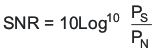
SNR is either given in units of dBc (dB to carrier) when the absolute power of the fundamental is used as the reference, or dBFS (dB to full-scale) when the power of the fundamental is extrapolated to the converter full-scale range.
Signal-to-Noise and Distortion (SINAD) – SINAD is the ratio of the power of the fundamental (PS) to the power of all the other spectral components including noise (PN) and distortion (PD), but excluding dc.
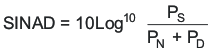
SINAD is either given in units of dBc (dB to carrier) when the absolute power of the fundamental is used as the reference, or dBFS (dB to full-scale) when the power of the fundamental is extrapolated to the converter full-scale range.
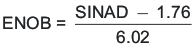
Effective Number of Bits (ENOB) – ENOB is a measure of the converter performance as compared to the theoretical limit based on quantization noise.
Total Harmonic Distortion (THD) – THD is the ratio of the power of the fundamental (PS) to the power of the first nine harmonics (PD).
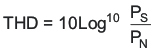
THD is typically given in units of dBc (dB to carrier).
Spurious-Free Dynamic Range (SFDR) – The ratio of the power of the fundamental to the highest other spectral component (either spur or harmonic). SFDR is typically given in units of dBc (dB to carrier).
Two-Tone Intermodulation Distortion – IMD3 is the ratio of the power of the fundamental (at frequencies f1 and f2) to the power of the worst spectral component at either frequency 2f1 – f2 or 2f2 – f1. IMD3 is either given in units of dBc (dB to carrier) when the absolute power of the fundamental is used as the reference, or dBFS (dB to full-scale) when the power of the fundamental is extrapolated to the converter full-scale range.
DC Power-Supply Rejection Ratio (DC PSRR) – DC PSSR is the ratio of the change in offset error to a change in analog supply voltage. The dc PSRR is typically given in units of mV/V.
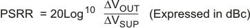
AC Power-Supply Rejection Ratio (AC PSRR) – AC PSRR is the measure of rejection of variations in the supply voltage by the ADC. If ΔVSUP is the change in supply voltage and ΔVOUT is the resultant change of the ADC output code (referred to the input), then:
Voltage Overload Recovery – The number of clock cycles taken to recover to less than 1% error after an overload on the analog inputs. This is tested by separately applying a sine wave signal with 6 dB positive and negative overload. The deviation of the first few samples after the overload (from the expected values) is noted.
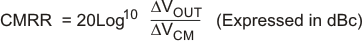
Common-Mode Rejection Ratio (CMRR) – CMRR is the measure of rejection of variation in the analog input common-mode by the ADC. If ΔVCM_IN is the change in the common-mode voltage of the input pins and ΔVOUT is the resulting change of the ADC output code (referred to the input), then:
Crosstalk (only for multi-channel ADCs) – This is a measure of the internal coupling of a signal from an adjacent channel into the channel of interest. It is specified separately for coupling from the immediate neighboring channel (near-channel) and for coupling from channel across the package (far-channel). It is usually measured by applying a full-scale signal in the adjacent channel. Crosstalk is the ratio of the power of the coupling signal (as measured at the output of the channel of interest) to the power of the signal applied at the adjacent channel input. It is typically expressed in dBc.