JAJSPW8E march   2011  – february 2023 ADS4222 , ADS4225 , ADS4226 , ADS4242 , ADS4245 , ADS4246

PRODUCTION DATA  

  1. 特長
  2. アプリケーション
  3. 概要
  4. Revision History
  5. 概要 (続き)
  6. Pin Configuration and Functions
    1.     Pin Functions – LVDS Mode
    2.     Pin Functions – CMOS Mode
  7. Specifications
    1. 7.1  Absolute Maximum Ratings
    2. 7.2  ESD Ratings
    3. 7.3  Recommended Operating Conditions
    4. 7.4  Thermal Information
    5. 7.5  Electrical Characteristics: ADS4246, ADS4245, ADS4242
    6. 7.6  Electrical Characteristics: ADS4226, ADS4225, ADS4222
    7. 7.7  Electrical Characteristics: General
    8. 7.8  Digital Characteristics
    9. 7.9  Timing Requirements: LVDS and CMOS Modes #GUID-C6C0701B-A11B-492F-BD6B-B774F5FE4665/SLAS6895399
    10. 7.10 Serial Interface Timing Characteristics #GUID-3852E7CE-C5B6-42F5-A56A-70AB1B981302/SBAS5097810
    11. 7.11 Reset Timing (Only When Serial Interface Is Used)
    12. 7.12 Typical Characteristics
      1. 7.12.1 ADS4246
      2. 7.12.2 ADS4245
      3. 7.12.3 ADS4242
      4. 7.12.4 ADS4226
      5. 7.12.5 ADS4225
      6. 7.12.6 ADS4222
      7. 7.12.7 General
      8. 7.12.8 Contour
  8. Detailed Description
    1. 8.1 Overview
    2. 8.2 Functional Block Diagrams
    3. 8.3 Feature Description
      1. 8.3.1 Analog Input
        1. 8.3.1.1 Drive Circuit Requirements
        2. 8.3.1.2 Driving Circuit
      2. 8.3.2 Clock Input
      3. 8.3.3 Digital Functions
      4. 8.3.4 Gain for SFDR/SNR Trade-off
      5. 8.3.5 Offset Correction
    4. 8.4 Device Functional Modes
      1. 8.4.1 Power-Down
        1. 8.4.1.1 Global Power-Down
        2. 8.4.1.2 Channel Standby
        3. 8.4.1.3 Input Clock Stop
    5. 8.5 Programming
      1. 8.5.1 47
      2. 8.5.2 Parallel Configuration Only
      3. 8.5.3 Serial Interface Configuration Only
      4. 8.5.4 Using Both Serial Interface and Parallel Controls
      5. 8.5.5 Parallel Configuration Details
      6. 8.5.6 Serial Interface Details
        1. 8.5.6.1 Register Initialization
        2. 8.5.6.2 Serial Register Readout
      7. 8.5.7 Digital Output Information
        1. 8.5.7.1 Output Interface
        2. 8.5.7.2 DDR LVDS Outputs
        3. 8.5.7.3 LVDS Buffer
        4. 8.5.7.4 Parallel CMOS Interface
        5. 8.5.7.5 CMOS Interface Power Dissipation
        6. 8.5.7.6 Multiplexed Mode of Operation
        7. 8.5.7.7 Output Data Format
    6. 8.6 Register Maps
      1. 8.6.1 64
      2. 8.6.2 Description Of Serial Registers
  9. Application and Implementation
    1. 9.1 Application Information
    2. 9.2 Typical Application
      1. 9.2.1 Design Requirements
      2. 9.2.2 Detailed Design Procedure
        1. 9.2.2.1 Analog Input
        2. 9.2.2.2 Clock Driver
        3. 9.2.2.3 Digital Interface
        4. 9.2.2.4 SNR and Clock Jitter
      3. 9.2.3 Application Curves
    3. 9.3 Power Supply Recommendations
      1. 9.3.1 Sharing DRVDD and AVDD Supplies
      2. 9.3.2 Using DC/DC Power Supplies
      3. 9.3.3 Power Supply Bypassing
    4. 9.4 Layout
      1. 9.4.1 Layout Guidelines
        1. 9.4.1.1 Grounding
        2. 9.4.1.2 Supply Decoupling
        3. 9.4.1.3 Exposed Pad
        4. 9.4.1.4 Routing Analog Inputs
      2. 9.4.2 Layout Example
  10. 10Device and Documentation Support
    1. 10.1 Device Support
      1. 10.1.1 Device Nomenclature
    2. 10.2 Documentation Support
      1. 10.2.1 Related Documentation
    3. 10.3 サポート・リソース
    4. 10.4 商標
    5. 10.5 静電気放電に関する注意事項
    6. 10.6 用語集
  11. 11Mechanical, Packaging, and Orderable Information

パッケージ・オプション

メカニカル・データ(パッケージ|ピン)
サーマルパッド・メカニカル・データ
発注情報

Clock Input

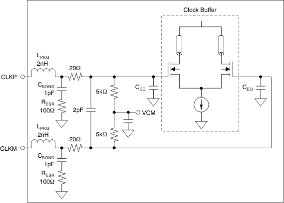
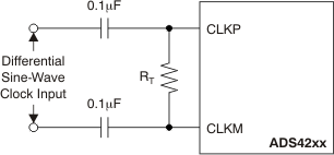
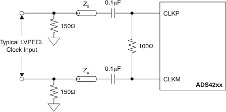
The ADS424x/422x clock inputs can be driven differentially (sine, LVPECL, or LVDS) or single-ended (LVCMOS), with little or no difference in performance between them. The common-mode voltage of the clock inputs is set to VCM using internal 5-kΩ resistors. This setting allows the use of transformer-coupled drive circuits for sine-wave clock or ac-coupling for LVPECL and LVDS clock sources are shown in Figure 8-10, Figure 8-11 and Figure 8-12. The internal clock buffer is shown in Figure 8-13.
GUID-752AAE67-C0F0-494F-A91D-A483F887521A-low.gif
RT = termination resister, if necessary.
Figure 8-10 Differential Sine-Wave Clock Driving Circuit
GUID-5CBB69A2-0E84-4F67-AFD5-9C897758E256-low.gifFigure 8-12 LVPECL Clock Driving Circuit
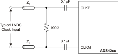
GUID-8B5E9E76-BEE9-4B54-A508-47D1A7407D1E-low.gifFigure 8-11 LVDS Clock Driving Circuit
GUID-743C7081-F94B-499B-AEF9-77AE5F074C14-low.gif
CEQ is 1 pF to 3 pF, and is the equivalent input capacitance of the clock buffer.
Figure 8-13 Internal Clock Buffer

A single-ended CMOS clock can be ac-coupled to the CLKP input, with CLKM connected to ground with a 0.1-μF capacitor, as shown in Figure 8-14. For best performance, the clock inputs must be driven differentially, thereby reducing susceptibility to common-mode noise. For high input frequency sampling, it is recommended to use a clock source with very low jitter. Band-pass filtering of the clock source can help reduce the effects of jitter. There is no change in performance with a non-50% duty cycle clock input.
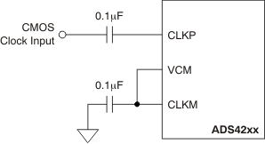
GUID-C824065C-567E-4F02-A89D-78837F977E55-low.gifFigure 8-14 Single-Ended Clock Driving Circuit