JAJSM94B June 2021 – June 2022 DAC12DL3200
PRODUCTION DATA
- 1 特長
- 2 アプリケーション
- 3 概要
- 4 Revision History
- 5 Pin Configuration and Functions
-
6 Specifications
- 6.1 Absolute Maximum Ratings
- 6.2 ESD Ratings
- 6.3 Recommended Operating Conditions
- 6.4 Thermal Information
- 6.5 Electrical Characteristics - DC Specifications
- 6.6 Electrical Characteristics - Power Consumption
- 6.7 Electrical Characteristics - AC Specifications
- 6.8 Timing Requirements
- 6.9 Switching Characteristics
- 6.10 Typical Characteristics
-
7 Detailed Description
- 7.1 Overview
- 7.2 Functional Block Diagram
- 7.3
Feature Description
- 7.3.1 DAC Output Modes
- 7.3.2 DAC Output Interface
- 7.3.3 LVDS Interface
- 7.3.4 Multi-Device Synchronization (SYSREF+/-)
- 7.3.5 Alarms
- 7.4 Device Functional Modes
- 7.5 Programming
- 8 Application and Implementation
- 9 Device and Documentation Support
- 10Mechanical, Packaging, and Orderable Information
パッケージ・オプション
メカニカル・データ(パッケージ|ピン)
サーマルパッド・メカニカル・データ
発注情報
7.3.3.1 MODE0: Two LVDS banks per channel
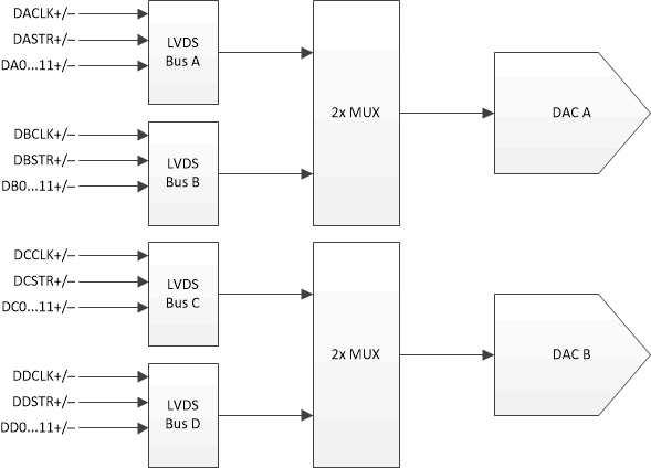
MODE0 uses two 12-bit LVDS data buses per channel. Due to the high bit rate, each 12-bit LVDS bus has its own dual-data rate (DDR) clock to maximize timing windows resulting in four total data clocks. This mode allows half of the maximum data rate into dual DACs. Table 7-4 shows the LVDS bus, data clock and strobe assignments for each channel. Figure 7-13 shows the block diagram for this mode for further understanding, including the signal assignments.
| DAC CHANNEL | LVDS BUSES | DATA CLOCKS | STROBE USED |
|---|---|---|---|
| A | A, B | DACLK, DBCLK | DASTR, DBSTR |
| B | C, D | DCCLK, DDCLK | DCSTR, DDSTR |
 Figure 7-13 MODE0 Block Diagram
Figure 7-14 shows the functional timing diagram for MODE0. Four 12-bit buses are used, with buses A and B for DAC channel A data and buses C and D for DAC channel B data. There is no strict timing skew requirement between LVDS buses (e.g. A to B or A to D) as long as the internal FIFOs maintain sufficient offset between read and write pointers.
Having the LVDS banks staggered as shown in Figure 7-14 allows the data from each bank to arrive as it is needed and results in minimal latency from each bank. If the LVDS banks have their clocks aligned, then the data on buses B and D are provided to the chip 1 DAC clocks before it is needed.