JAJSED2B August 2017 – January 2018 DAC5672A
PRODUCTION DATA.
- 1 特長
- 2 アプリケーション
- 3 概要
- 4 改訂履歴
- 5 Pin Configuration and Functions
-
6 Specifications
- 6.1 Absolute Maximum Ratings
- 6.2 ESD Ratings
- 6.3 Recommended Operating Conditions
- 6.4 Thermal Information
- 6.5 Electrical Characteristics
- 6.6 Electrical Characteristics
- 6.7 Electrical Characteristics: AC Characteristics
- 6.8 Electrical Characteristics: Digital Characteristics
- 6.9 Switching Characteristics
- 6.10 Typical Characteristics
- 7 Detailed Description
- 8 Application and Implementation
- 9 Power Supply Recommendations
- 10Layout
- 11デバイスおよびドキュメントのサポート
- 12メカニカル、パッケージ、および注文情報
7.5.1.1 Digital Inputs
The data input ports of the DAC5672A accept a standard positive coding with data bits DA13 and DB13 being the most significant bits (MSB). The converter outputs support a clock rate of up to 275 MSPS. The best performance is typically achieved with a symmetric duty cycle for write and clock; however, the duty cycle may vary as long as the timing specifications are met. Similarly, the setup and hold times may be chosen within their specified limits.
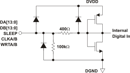
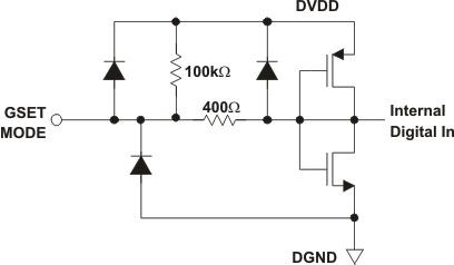
All digital inputs of the DAC5672A are CMOS compatible. Figure 23 and Figure 24 show schematics of the equivalent CMOS digital inputs of the DAC5672A. The pullup and pulldown circuitry is approximately equivalent to 100 kΩ. The 14-bit digital data input follows the offset positive binary coding scheme. The DAC5672A is designed to operate with a digital supply (DVDD) of 3 V to 3.6 V.

