JAJSDY1C June 2017 – March 2018 TPS25740B
PRODUCTION DATA.
- 1 特長
- 2 アプリケーション
- 3 概要
- 4 改訂履歴
- 5 概要(続き)
- 6 Device Comparison Table
- 7 Pin Configuration and Functions
- 8 Specifications
-
9 Detailed Description
- 9.1 Overview
- 9.2 Functional Block Diagram
- 9.3
Feature Description
- 9.3.1 ENSRC
- 9.3.2 USB Type-C CC Logic (CC1, CC2)
- 9.3.3 USB PD BMC Transmission (CC1, CC2, VTX)
- 9.3.4 USB PD BMC Reception (CC1, CC2)
- 9.3.5 Discharging (DSCG, VPWR)
- 9.3.6 Configuring Voltage Capabilities (HIPWR)
- 9.3.7 Configuring Power Capabilities (PSEL, PCTRL, HIPWR)
- 9.3.8 Gate Driver (GDNG, GDNS)
- 9.3.9 Fault Monitoring and Protection
- 9.3.10 Voltage Control (CTL1, CTL2,CTL3)
- 9.3.11 Sink Attachment Indicator (DVDD)
- 9.3.12 Power Supplies (VAUX, VDD, VPWR, DVDD)
- 9.3.13 Grounds (AGND, GND)
- 9.3.14 Output Power Supply (DVDD)
- 9.4 Device Functional Modes
-
10Application and Implementation
- 10.1
Application Information
- 10.1.1 System-Level ESD Protection
- 10.1.2 Using ENSRC to Enable the Power Supply upon Sink Attachment
- 10.1.3 Use of GD Internal Clamp
- 10.1.4 Resistor Divider on GD for Programmable Start Up
- 10.1.5 Selection of the CTL1, CTL2, and CTL3 Resistors (R(FBL1), R(FBL2), and R(FBL3))
- 10.1.6 Voltage Transition Requirements
- 10.1.7 VBUS Slew Control using GDNG C(SLEW)
- 10.1.8 Tuning OCP using RF and CF
- 10.2 Typical Applications
- 10.3 System Examples
- 10.1
Application Information
- 11Power Supply Recommendations
- 12Layout
- 13デバイスおよびドキュメントのサポート
- 14メカニカル、パッケージ、および注文情報
パッケージ・オプション
メカニカル・データ(パッケージ|ピン)
- RGE|24
サーマルパッド・メカニカル・データ
- RGE|24
発注情報
9.3.2 USB Type-C CC Logic (CC1, CC2)
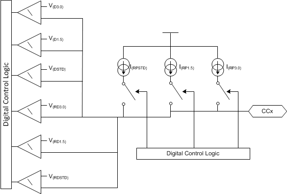
The device uses a current source to implement the pull up resistance USB Type-C requires for Sources. While waiting for a valid connection, the device applies a default pullup of I(RPSTD). A sink attachment is detected when the voltage on one (not both) of the CC pins remains between V(RDSTD) and V(DSTD) for tCcDeb and the voltage on the VBUS pin is below V(VBUS_FTH). Then after turning on VBUS and disabling the Rp current source for the CCx pin not connected through the cable, the device applies I(RP3.0) to advertise 3 A to non-PD sinks. Finally, if it is determined that the attached sink is PD-capable, the device applies I(RP1.5). During this sequence if the voltage on the monitored CC pin exceeds the detach threshold then the device removes VBUS and begins watching for a sink attachment again.
The TPS25740B digital logic selects the current source switch as illustrated in Figure 23. The schematic shown is replicated for each CC pin.
 Figure 23. USB Type-C Rp Current Sources and Detection Comparators
 If the voltage on both CC pins remains above V(RDSTD) for tCcDeb, then the device goes to the sleep mode. In the sleep mode a less accurate current source is applied and a less accurate comparator watches for attachment (see V(WAKE), and I(DSDFP)).