JAJSDY1C June 2017 – March 2018 TPS25740B
PRODUCTION DATA.
- 1 特長
- 2 アプリケーション
- 3 概要
- 4 改訂履歴
- 5 概要(続き)
- 6 Device Comparison Table
- 7 Pin Configuration and Functions
- 8 Specifications
-
9 Detailed Description
- 9.1 Overview
- 9.2 Functional Block Diagram
- 9.3
Feature Description
- 9.3.1 ENSRC
- 9.3.2 USB Type-C CC Logic (CC1, CC2)
- 9.3.3 USB PD BMC Transmission (CC1, CC2, VTX)
- 9.3.4 USB PD BMC Reception (CC1, CC2)
- 9.3.5 Discharging (DSCG, VPWR)
- 9.3.6 Configuring Voltage Capabilities (HIPWR)
- 9.3.7 Configuring Power Capabilities (PSEL, PCTRL, HIPWR)
- 9.3.8 Gate Driver (GDNG, GDNS)
- 9.3.9 Fault Monitoring and Protection
- 9.3.10 Voltage Control (CTL1, CTL2,CTL3)
- 9.3.11 Sink Attachment Indicator (DVDD)
- 9.3.12 Power Supplies (VAUX, VDD, VPWR, DVDD)
- 9.3.13 Grounds (AGND, GND)
- 9.3.14 Output Power Supply (DVDD)
- 9.4 Device Functional Modes
-
10Application and Implementation
- 10.1
Application Information
- 10.1.1 System-Level ESD Protection
- 10.1.2 Using ENSRC to Enable the Power Supply upon Sink Attachment
- 10.1.3 Use of GD Internal Clamp
- 10.1.4 Resistor Divider on GD for Programmable Start Up
- 10.1.5 Selection of the CTL1, CTL2, and CTL3 Resistors (R(FBL1), R(FBL2), and R(FBL3))
- 10.1.6 Voltage Transition Requirements
- 10.1.7 VBUS Slew Control using GDNG C(SLEW)
- 10.1.8 Tuning OCP using RF and CF
- 10.2 Typical Applications
- 10.3 System Examples
- 10.1
Application Information
- 11Power Supply Recommendations
- 12Layout
- 13デバイスおよびドキュメントのサポート
- 14メカニカル、パッケージ、および注文情報
パッケージ・オプション
メカニカル・データ(パッケージ|ピン)
- RGE|24
サーマルパッド・メカニカル・データ
- RGE|24
発注情報
9.3.9.3 System Fault Input (GD, VPWR)
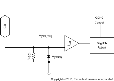
The gate-driver disable pin provides a method of overriding the internal control of GDNG and GDNS. A falling edge on GD disables the gate driver within tGDoff. If GD is held low after a sink is attached for 600 ms then a hard reset will be generated and the device sends a hard reset and go through its startup process again.
The GD input can be controlled by a voltage or current source. An internal voltage clamp is provided to limit the input voltage in current source applications. The clamp can safely conduct up to 80 µA and will remain high impedance up to 6.5 V before clamping.
 Figure 36. Overcurrent Protection Circuit, (GD)
 If the VPWR pin remains below its falling UVLO threshold (V(VPWR_TH)) for more than 600 ms after a sink is attached then the devices consider it a fault and will not enable GDNG. If the VPWR pin is between the rising and falling UVLO threshold, the device may enable GDNG and proceed with normal operations. However, after GDNG is enabled, if the VBUS pin does not rise above its UVLO within 190 ms the devices consider it a fast-shutdown fault and disables GDNG. Therefore, in order to ensure USB Type-C compliance and normal operation, the VPWR pin must be above its rising UVLO threshold (V(VPWR_TH)) within 275 ms of when ENSRC is pulled low and the VBUS pin must be above V(VBUS_RTH) within 190 ms of GDNG being enabled.