JAJSDY1C June 2017 – March 2018 TPS25740B
PRODUCTION DATA.
- 1 特長
- 2 アプリケーション
- 3 概要
- 4 改訂履歴
- 5 概要(続き)
- 6 Device Comparison Table
- 7 Pin Configuration and Functions
- 8 Specifications
-
9 Detailed Description
- 9.1 Overview
- 9.2 Functional Block Diagram
- 9.3
Feature Description
- 9.3.1 ENSRC
- 9.3.2 USB Type-C CC Logic (CC1, CC2)
- 9.3.3 USB PD BMC Transmission (CC1, CC2, VTX)
- 9.3.4 USB PD BMC Reception (CC1, CC2)
- 9.3.5 Discharging (DSCG, VPWR)
- 9.3.6 Configuring Voltage Capabilities (HIPWR)
- 9.3.7 Configuring Power Capabilities (PSEL, PCTRL, HIPWR)
- 9.3.8 Gate Driver (GDNG, GDNS)
- 9.3.9 Fault Monitoring and Protection
- 9.3.10 Voltage Control (CTL1, CTL2,CTL3)
- 9.3.11 Sink Attachment Indicator (DVDD)
- 9.3.12 Power Supplies (VAUX, VDD, VPWR, DVDD)
- 9.3.13 Grounds (AGND, GND)
- 9.3.14 Output Power Supply (DVDD)
- 9.4 Device Functional Modes
-
10Application and Implementation
- 10.1
Application Information
- 10.1.1 System-Level ESD Protection
- 10.1.2 Using ENSRC to Enable the Power Supply upon Sink Attachment
- 10.1.3 Use of GD Internal Clamp
- 10.1.4 Resistor Divider on GD for Programmable Start Up
- 10.1.5 Selection of the CTL1, CTL2, and CTL3 Resistors (R(FBL1), R(FBL2), and R(FBL3))
- 10.1.6 Voltage Transition Requirements
- 10.1.7 VBUS Slew Control using GDNG C(SLEW)
- 10.1.8 Tuning OCP using RF and CF
- 10.2 Typical Applications
- 10.3 System Examples
- 10.1
Application Information
- 11Power Supply Recommendations
- 12Layout
- 13デバイスおよびドキュメントのサポート
- 14メカニカル、パッケージ、および注文情報
パッケージ・オプション
メカニカル・データ(パッケージ|ピン)
- RGE|24
サーマルパッド・メカニカル・データ
- RGE|24
発注情報
9.3.3 USB PD BMC Transmission (CC1, CC2, VTX)
An example of the BMC signal, specifically the end of the preamble and beginning of start-of-packet (SOP) is shown below. There is always an edge at the end of each bit or unit interval, and ones have an edge half way through the unit interval.
 Figure 24. BMC Encoded End of Preamble, Beginning of SOP
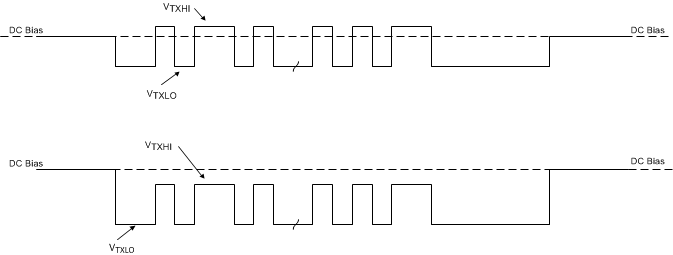
 While engaging in USB PD communications, the device is applying I(RP1.5) or I(RP3.0), so the CC line has a DC voltage of 0.918 V or 1.68 V, respectively. When the BMC signal is transmitted on the CC line, the transmitter overrides this DC voltage as shown in Figure 25. The transmitter bias rail (VTX) is internally generated and may not be used for any other purpose in the system. The VTX pin is only high while the TPS25740B is transmitting a USB PD message.
 Figure 25. USB PD BMC Transmission on the CC Line
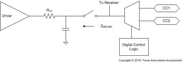
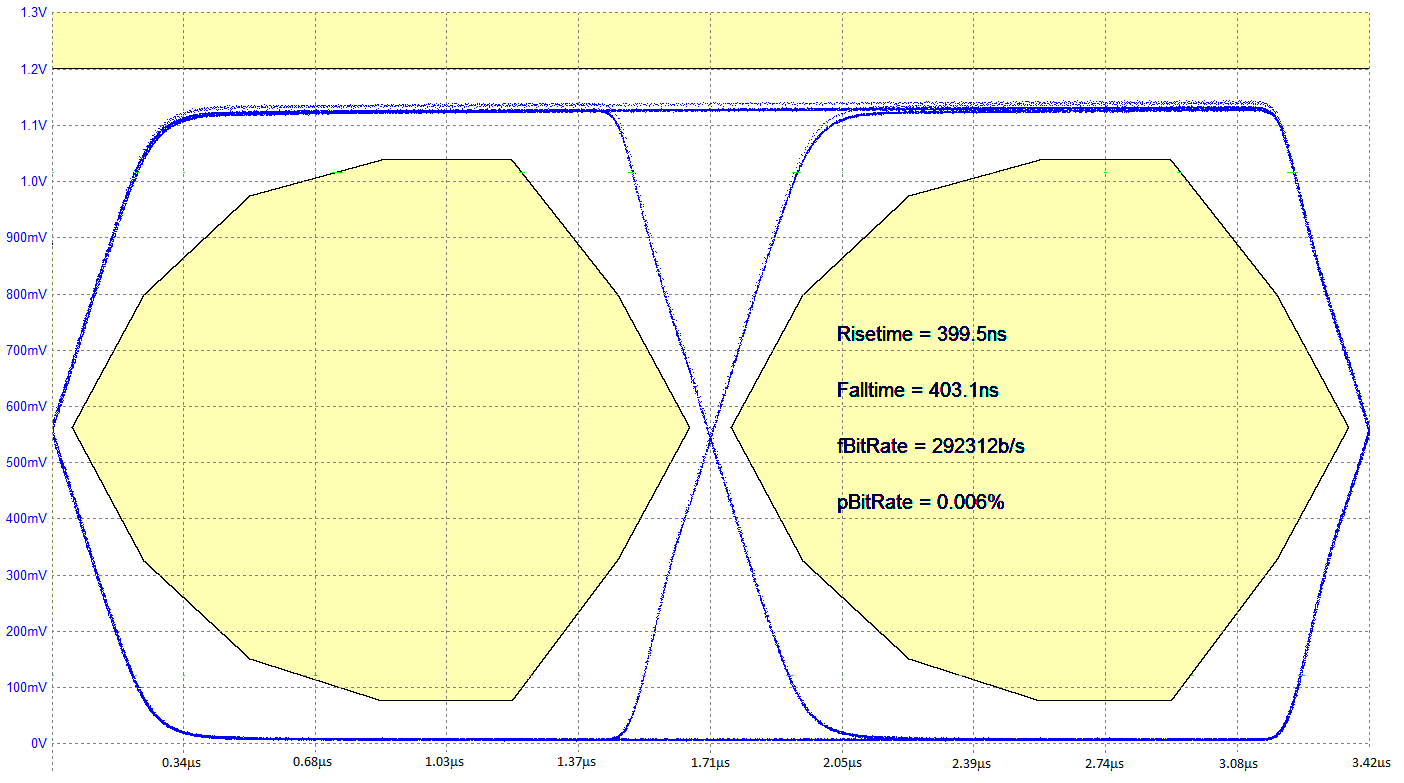
 The device transmissions meet the eye diagram USB PD requirements (refer to USB PD in ドキュメントのサポート) across the recommended temperature range. Figure 26 shows the transmitter schematic.
 Figure 26. USB PD BMC Transmitter Schematic
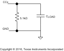
 The transmit eye diagram shown in Figure 28 was measured using the test load shown in Figure 27 with a CLOAD within the allowed range. The total capacitance CLOAD is computed as:
Where:
- 200 pF < C(RX) < 600 pF
- CCablePlug < 25 pF
- Ca < 625 pF
- 200 pF < CReceiver < 600 pF
Therefore, 400 pF < CLOAD < 1850 pF.
 Figure 27. Test Load for BMC Transmitter
 Figure 28 shows the transmit eye diagram for the TPS25740B.
 Figure 28. Transmit Eye Diagram (BMC)