JAJSMF3A May 2022 – September 2022 TPS25985
PRODUCTION DATA
- 1 特長
- 2 アプリケーション
- 3 概要
- 4 Revision History
- 5 概要 (続き)
- 6 Pin Configuration and Functions
- 7 Specifications
-
8 Detailed Description
- 8.1 Overview
- 8.2 Functional Block Diagram
- 8.3
Feature Description
- 8.3.1 Undervoltage Protection
- 8.3.2 Insertion Delay
- 8.3.3 Overvoltage Protection
- 8.3.4 Inrush Current, Overcurrent, and Short-Circuit Protection
- 8.3.5 Analog Load Current Monitor (IMON)
- 8.3.6 Mode Selection (MODE)
- 8.3.7 Parallel Device Synchronization (SWEN)
- 8.3.8 Stacking Multiple eFuses for Unlimited Scalability
- 8.3.9 Analog Junction Temperature Monitor (TEMP)
- 8.3.10 Overtemperature Protection
- 8.3.11 Fault Response and Indication (FLT)
- 8.3.12 Power Good Indication (PG)
- 8.3.13 Output Discharge
- 8.3.14 General Purpose Comparator
- 8.3.15 FET Health Monitoring
- 8.3.16 Single Point Failure Mitigation
- 8.4 Device Functional Modes
- 9 Application and Implementation
- 10Power Supply Recommendations
- 11Layout
- 12Device and Documentation Support
- 13Mechanical, Packaging, and Orderable Information
8.3.12 Power Good Indication (PG)
Power Good indication is an active high output which is asserted high to indicate when the device is in steady-state and capable of delivering maximum power.
Event or Condition | FET Status | PG Pin Status | PG Delay |
|---|---|---|---|
Undervoltage ( VEN < VUVLO) | OFF | L | tPGD |
| VIN < VUVP | OFF | L | |
| VDD < VUVP | OFF | L | |
Overvoltage (VIN > VOVP) | OFF | L | tPGD |
Steady-state | ON | H | tPGA |
Inrush | ON | L | tPGA |
Transient overcurrent | ON | H | N/A |
Circuit-breaker (persistent overcurrent followed by ITIMER expiry) | OFF | L (MODE = H) H (MODE = L) | tPGD N/A |
Fast-trip | OFF | L (MODE = H) H (MODE = L) | tPGD N/A |
ILM pin open | OFF | L (MODE = H) H (MODE = L) | tITIMER + tPGD N/A |
ILM pin short | OFF | L (MODE = H) H(MODE = L) | tPGD N/A |
Overtemperature | Shutdown | L (MODE = H) H (MODE = L) | tPGD N/A |
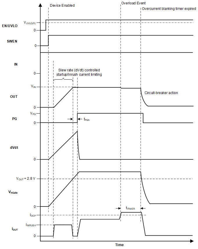
After power up, PG is pulled low initially. The device initiates an inrush sequence in which the gate driver circuit starts charging the gate capacitance from the internal charge pump. When the FET gate voltage reaches the full overdrive indicating that the inrush sequence is complete and the device is capable of delivering full power, the PG pin is asserted HIGH after a de-glitch time (tPGA).
The PG is de-asserted if the FET is turned off at any time during normal operation. The PG de-assertion de-glitch time is tPGD.
 Figure 8-8 TPS25985x PG Timing Diagram
The PG is an open-drain pin and must be pulled up to an external supply.
When there is no supply to the device, the PG pin is expected to stay low. However, there is no active pulldown in this condition to drive this pin all the way down to 0 V. If the PG pin is pulled up to an independent supply which is present even if the device is unpowered, there can be a small voltage seen on this pin depending on the pin sink current, which is a function of the pullup supply voltage and resistor. Minimize the sink current to keep this pin voltage low enough not to be detected as a logic HIGH by associated external circuits in this condition.
When the device is used in secondary mode (MODE = GND) in conjunction with another TPS25985 device as a primary device in a parallel chain, it controls the PG assertion during start-up, but after the device reaches steady-state, it no longer has control over the PG de-assertion. Refer to the Mode Selection (MODE) for more details.