JAJSMF3A May 2022 – September 2022 TPS25985
PRODUCTION DATA
- 1 特長
- 2 アプリケーション
- 3 概要
- 4 Revision History
- 5 概要 (続き)
- 6 Pin Configuration and Functions
- 7 Specifications
-
8 Detailed Description
- 8.1 Overview
- 8.2 Functional Block Diagram
- 8.3
Feature Description
- 8.3.1 Undervoltage Protection
- 8.3.2 Insertion Delay
- 8.3.3 Overvoltage Protection
- 8.3.4 Inrush Current, Overcurrent, and Short-Circuit Protection
- 8.3.5 Analog Load Current Monitor (IMON)
- 8.3.6 Mode Selection (MODE)
- 8.3.7 Parallel Device Synchronization (SWEN)
- 8.3.8 Stacking Multiple eFuses for Unlimited Scalability
- 8.3.9 Analog Junction Temperature Monitor (TEMP)
- 8.3.10 Overtemperature Protection
- 8.3.11 Fault Response and Indication (FLT)
- 8.3.12 Power Good Indication (PG)
- 8.3.13 Output Discharge
- 8.3.14 General Purpose Comparator
- 8.3.15 FET Health Monitoring
- 8.3.16 Single Point Failure Mitigation
- 8.4 Device Functional Modes
- 9 Application and Implementation
- 10Power Supply Recommendations
- 11Layout
- 12Device and Documentation Support
- 13Mechanical, Packaging, and Orderable Information
6 Pin Configuration and Functions
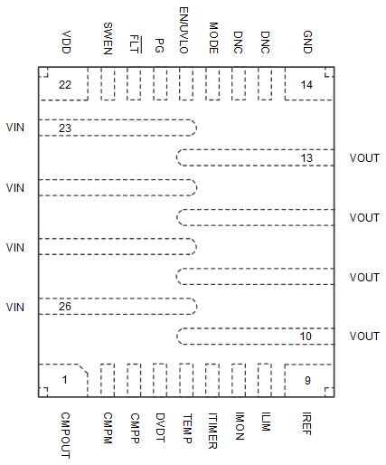
 Figure 6-1 TPS25985x RQP Package 26-pin QFN Top View
PIN | TYPE | DESCRIPTION | |
|---|---|---|---|
NAME | NO. | ||
CMPOUT | 1 | O | General purpose comparator open-drain output |
CMPM | 2 | I | General purpose comparator negative input |
CMPP | 3 | I | General purpose comparator positive input |
DVDT | 4 | I/O | Start-up output slew rate control pin. Leave this pin open to allow fastest start-up. Connect capacitor to ground to slow down the slew rate to manage inrush current. |
TEMP | 5 | O | Die junction temperature monitor analog voltage output. Can be tied together with TEMP outputs of multiple devices in a parallel configuration to indicate the peak temperature of the chain. |
ITIMER | 6 | I/O | A capacitor from this pin to GND sets the overcurrent blanking interval during which the output current can temporarily exceed the overcurrent threshold (but lower than fast-trip threshold) during steady-state operation before the device overcurrent response takes action. |
IMON | 7 | O | An external resistor from this pin to GND sets the overcurrent protection threshold and fast-trip threshold during steady-state. This pin also acts as a fast and accurate analog output load current monitor signal during steady-state. Do not leave floating. |
ILIM | 8 | O | An external resistor from this pin to GND sets the current limit threshold and fast-trip threshold during start-up. This also sets the active current sharing threshold during steady-state. Do not leave floating. |
IREF | 9 | I/O | Reference voltage for overcurrent, short-circuit protection and active current sharing blocks. Can be generated using internal current source and resistor on this pin, or can be driven from external voltage source. Do not leave floating. |
OUT | 10, 11, 12, 13 | P | Power output. Must be soldered to output power plane uniformly to ensure proper heat dissipation and to maintain optimal current distribution through the device. |
GND | 14 | G | Device ground reference pin. Connect to system ground. |
DNC | 15 | X | Do not connect anything to this pin. |
DNC | 16 | X | Do not connect anything to this pin. |
MODE | 17 | I | MODE selection pin. Leave the pin floating for standalone and primary mode of operation. Connect the pin to GND to configure device as a secondary device in a parallel chain. |
EN/UVLO | 18 | I | Active high enable input. Connect resistor divider from input supply to set the undervoltage threshold. Do not leave floating. |
PG | 19 | I/O | Open-drain active high Power Good indication |
FLT | 20 | O | Open-drain active low fault indication |
SWEN | 21 | I/O | Open-drain signal to indicate and control power switch ON/OFF status. This pin facilitates active synchronization between multiple devices in a parallel chain. |
VDD | 22 | P | Controller power input pin. Can be used to power the internal control circuitry with a filtered and stable supply which is not affected by system transients. Connect this pin to VIN through a series resistor and add a decoupling capacitor to GND. |
IN | 23, 24, 25, 26 | P | Power input. Must be soldered to input power plane uniformly to ensure proper heat dissipation and to maintain optimal current distribution through the device. |