JAJSMF3A May 2022 – September 2022 TPS25985
PRODUCTION DATA
- 1 特長
- 2 アプリケーション
- 3 概要
- 4 Revision History
- 5 概要 (続き)
- 6 Pin Configuration and Functions
- 7 Specifications
-
8 Detailed Description
- 8.1 Overview
- 8.2 Functional Block Diagram
- 8.3
Feature Description
- 8.3.1 Undervoltage Protection
- 8.3.2 Insertion Delay
- 8.3.3 Overvoltage Protection
- 8.3.4 Inrush Current, Overcurrent, and Short-Circuit Protection
- 8.3.5 Analog Load Current Monitor (IMON)
- 8.3.6 Mode Selection (MODE)
- 8.3.7 Parallel Device Synchronization (SWEN)
- 8.3.8 Stacking Multiple eFuses for Unlimited Scalability
- 8.3.9 Analog Junction Temperature Monitor (TEMP)
- 8.3.10 Overtemperature Protection
- 8.3.11 Fault Response and Indication (FLT)
- 8.3.12 Power Good Indication (PG)
- 8.3.13 Output Discharge
- 8.3.14 General Purpose Comparator
- 8.3.15 FET Health Monitoring
- 8.3.16 Single Point Failure Mitigation
- 8.4 Device Functional Modes
- 9 Application and Implementation
- 10Power Supply Recommendations
- 11Layout
- 12Device and Documentation Support
- 13Mechanical, Packaging, and Orderable Information
8.3.8 Stacking Multiple eFuses for Unlimited Scalability
For systems needing higher current than supported by a single TPS25985x, multiple TPS25985x devices can be connected in parallel to deliver the total system current. Conventional eFuses can not share current equally between themselves during steady-state due to mismatches in their path resistances (which includes the individual device RDSON variation from part to part, as well as the parasitic PCB trace resistance). This fact can lead to multiple problems in the system:
Some devices always carry higher current as compared to other devices, which can result in accelerated failures in those devices and an overall reduction in system operational lifetime.
As a result, thermal hotspots form on the board, devices, traces, and vias carrying higher current, leading to reliability concerns for the PCB. In addition, this problem makes thermal modeling and board thermal management more challenging for designers.
The devices carrying higher current can hit their individual circuit-breaker threshold prematurely even while the total system load current is lower than the overall circuit-breaker threshold. This action can lead to false tripping of the eFuse during normal operation. This has the effect of lowering the current-carrying capability of the parallel chain. In other words, the current rating of the parallel eFuse chain must be de-rated as compared to the sum of the current ratings of the individual eFuses. This de-rating factor is a function of the path resistance mismatch, the number of devices in parallel, and the individual eFuse circuit-breaker accuracy.
The need for de-rating has an adverse impact on the system design. The designer is forced to make one of these trade-offs:
Limit the operating load current of the system to below the derated current threshold of the eFuse chain. Essentially, it means lower platform capabilities than are supported by the power supply (PSU).
Increase the overall circuit-breaker threshold to allow the desired system load current to pass through without tripping. As a consequence, the power supply (PSU) must be oversized to deliver higher currents during faults to account for the de-grading of the overall circuit-breaker accuracy.
In either case, the system suffers from poor power supply utilization, which can mean sub-optimal system throughput or increased installation and operating costs, or both.
The TPS25985x uses a proprietary technique to address these problems and provide unlimited scalability of the solution by paralleling as many eFuses as needed. This is incorporated without unequal current sharing or any degradation in accuracy.
For this scheme to work correctly, the devices must be connected in the following manner:
The SWEN pins of all the devices are connected together.
The IMON pins of all the devices must be connected together. The RIMON resistor value on the combined IMON pin can be calculated using Equation 14.
Equation 14.
The RILIM for each individual eFuse must be selected based on Equation 34.
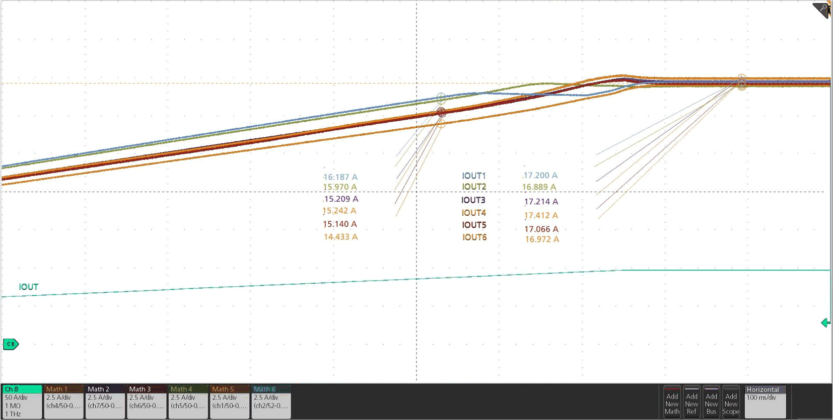
Equation 15.Where N = number of devices in parallel chain. Figure 8-7 illustrates the response of the active current sharing block in TPS25985 eFuse during steady-state.

| Intentional skew is introduced between the power path resistances for six devices and the load current is ramped up slowly. Equal current distribution is seen between all devices after the current through each device exceeds the active current sharing threshold. |
The active current sharing scheme is engaged when the current through any eFuse while in steady-state exceeds the individual current sharing threshold set by the RILIM based on Equation 16.
The active current sharing scheme is disengaged when the total system current exceeds the system overcurrent (circuit-breaker) threshold (IOCP(TOTAL)).