JAJSK13C September 2020 – December 2021 TPS542A52
PRODUCTION DATA
- 1 特長
- 2 アプリケーション
- 3 概要
- 4 Revision History
- 5 Pin Configuration and Functions
- 6 Specifications
-
7 Detailed Description
- 7.1 Overview
- 7.2 Functional Block Diagram
- 7.3
Feature Description
- 7.3.1 Enable and Adjustable Undervoltage Lockout
- 7.3.2 Input and VREG Undervoltage Lockout Protection
- 7.3.3 Voltage Reference and Setting the Output Voltage
- 7.3.4 Remote Sense Function
- 7.3.5 Switching Frequency
- 7.3.6 Voltage Control Mode Internal Compensation
- 7.3.7 Soft Start and Prebiased Output Start-up
- 7.3.8 Power Good
- 7.3.9 Overvoltage and Undervoltage Protection
- 7.3.10 Overcurrent Protection
- 7.3.11 High-Side FET Throttling
- 7.3.12 Overtemperature Protection
- 7.4 Device Functional Modes
-
8 Application and Implementation
- 8.1 Application Information
- 8.2
Typical Application
- 8.2.1
Full Analog Configuration
- 8.2.1.1 Design Requirements
- 8.2.1.2
Detailed Design Procedure
- 8.2.1.2.1 Custom Design With WEBENCH® Tools
- 8.2.1.2.2 Output Voltage Calculation
- 8.2.1.2.3 Switching Frequency Selection
- 8.2.1.2.4 Inductor Selection
- 8.2.1.2.5 Input Capacitor Selection
- 8.2.1.2.6 Bootstrap Capacitor Selection
- 8.2.1.2.7 R-C Snubber and VIN Pin High-Frequency Bypass
- 8.2.1.2.8 Output Capacitor Selection
- 8.2.1.2.9 Response to a Load Transient
- 8.2.1.2.10 Pin-Strap Setting
- 8.2.1.3 Application Curves
- 8.2.1.4 Typical Application Circuits
- 8.2.1
Full Analog Configuration
- 9 Power Supply Recommendations
- 10Layout
- 11Device and Documentation Support
- 12Mechanical, Packaging, and Orderable Information
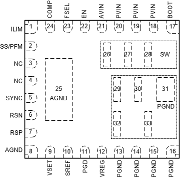
5 Pin Configuration and Functions
 Figure 5-1 RJM
Package33-Pin VQFNTop View
Figure 5-1 RJM
Package33-Pin VQFNTop ViewTable 5-1 Pin Functions
| PIN | I/O | DESCRIPTION | |
|---|---|---|---|
| NAME | NO. | ||
| AGND | 8, 25 | G | Ground of the internal analog and digital circuitry |
| AVIN | 21 | P | Power input to the controller. Tie this pin to PVIN. It is best to use an RC filter from PVIN such as 10-Ω and 100 nF to 1 μF. |
| BOOT | 17 | P | Gate drive voltage for high-side FET. Connect a bootstrap capacitor between this pin and SW. |
| COMP | 24 | I | A resistor to ground sets the compensation network. This pin can be grounded to select the default compensation and reduce BOM count. |
| EN | 22 | I | Enable pin. Float to enable, enable/disable with an external signal, or adjust the input undervoltage lockout with a resistor divider. |
| FSEL | 23 | I | A resistor to ground sets the switching frequency of the converter. This pin can be grounded to select the default switching frequency to reduce BOM count. |
| ILIM | 1 | I | A resistor to ground sets the overcurrent protection limit. This pin can be grounded to select default settings and reduce BOM count. |
| PGD | 11 | O | Open-drain power good status |
| PGND | 13-16, 29-33 | G | Power ground. These pins are internally connected to the return of the internal low-side FET. |
| PVIN | 18-20 | P | Power inputs to the power stage. Low impedance bypassing of these pins to PGND is critical. At least 10 nF to 100 nF capacitor from PVIN to PGND is required. |
| RSN | 6 | I | Remote sense ground return |
| RSP | 7 | I | Remote sense connection to VOUT |
| NC | 3 | N/A | No connect |
| NC | 4 | N/A | No connect |
| SREF | 10 | O | 1.2-V nominal system reference |
| SS/PFM | 2 | I | A resistor to ground sets the soft-start slew rate and PFM mode. To reduce BOM count, this pin can be grounded to use the default soft-start rate and enable PFM mode. |
| SYNC | 5 | I | This pin is a clock input for synchronizing the oscillator. |
| SW | 26-28 | O | Switch node output of the converter. Connect this pin to the output inductor to ground. |
| VREG | 12 | I/O | Bypass pin for the internal power stage LDO. It is recommended to use a 4.7-μF ceramic capacitor. |
| VSET | 9 | I | Output voltage reference for the control loop. This must be the mid-point of a resistive divider from SREF to AGND. Set this voltage to be 1/5 of the desired VOUT. |